Apparatus and methods for forming a modulation doped non-planar transistor

a technology of modulation doped non-planar transistors and apparatuses, which is applied in the direction of semiconductor devices, electrical apparatus, basic electric elements, etc., can solve the problem of incompatibility with previous non-planar transistor fabrication techniques

Inactive Publication Date: 2011-03-29
INTEL CORP
View PDF3 Cites 17 Cited by
  • Summary
  • Abstract
  • Description
  • Claims
  • Application Information

AI Technical Summary

Problems solved by technology

High mobility, modulation doped quantum well devices require the formation of several perpendicular epitaxially grown layers, making them incompatible with previous non-planar transistor fabrication techniques.

Method used


Image

  • Apparatus and methods for forming a modulation doped non-planar transistor
  • Apparatus and methods for forming a modulation doped non-planar transistor
  • Apparatus and methods for forming a modulation doped non-planar transistor

Examples


Embodiment Construction

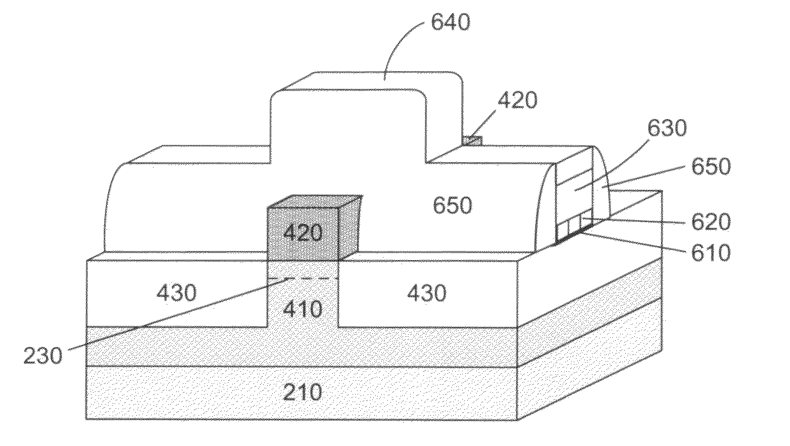
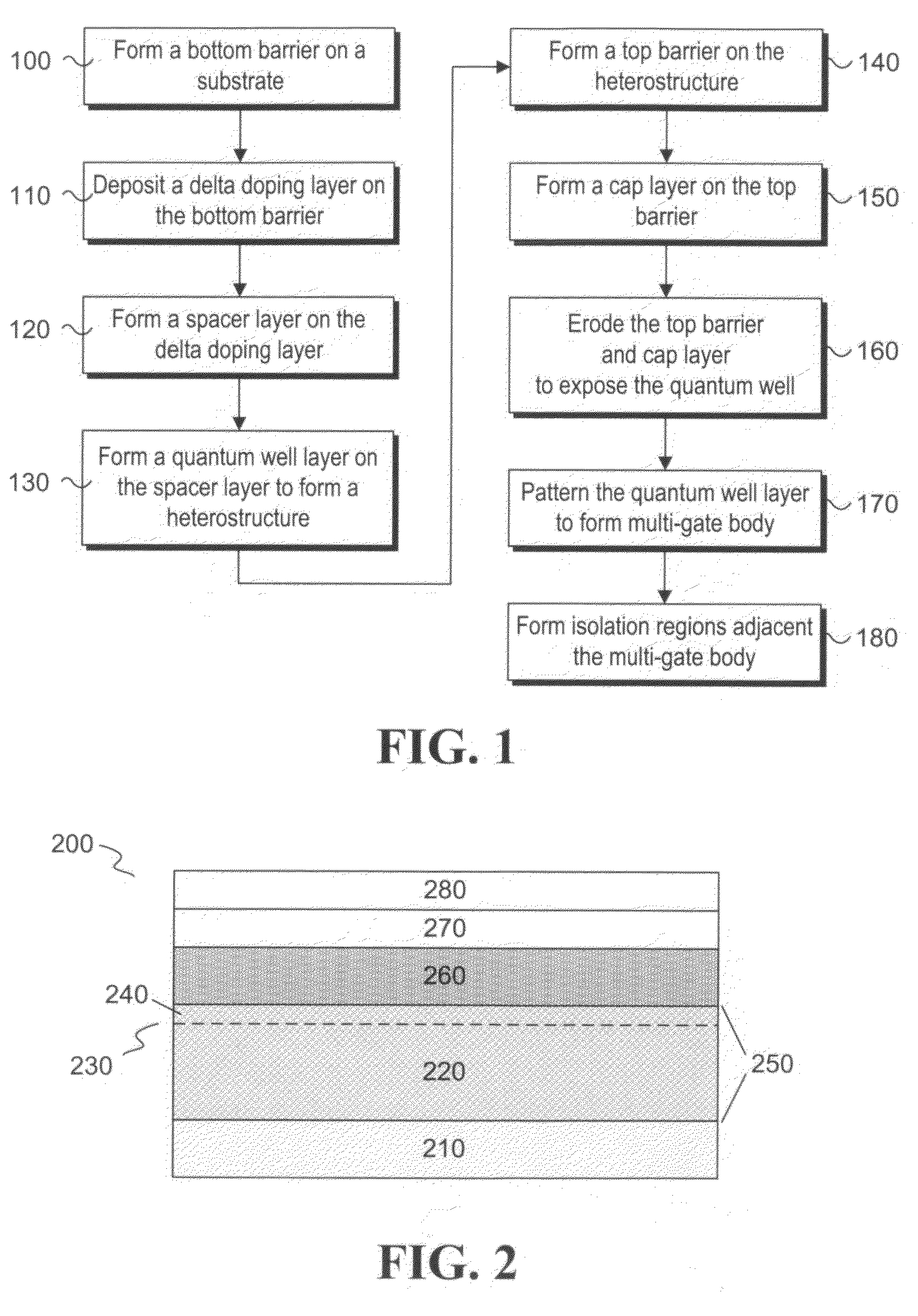
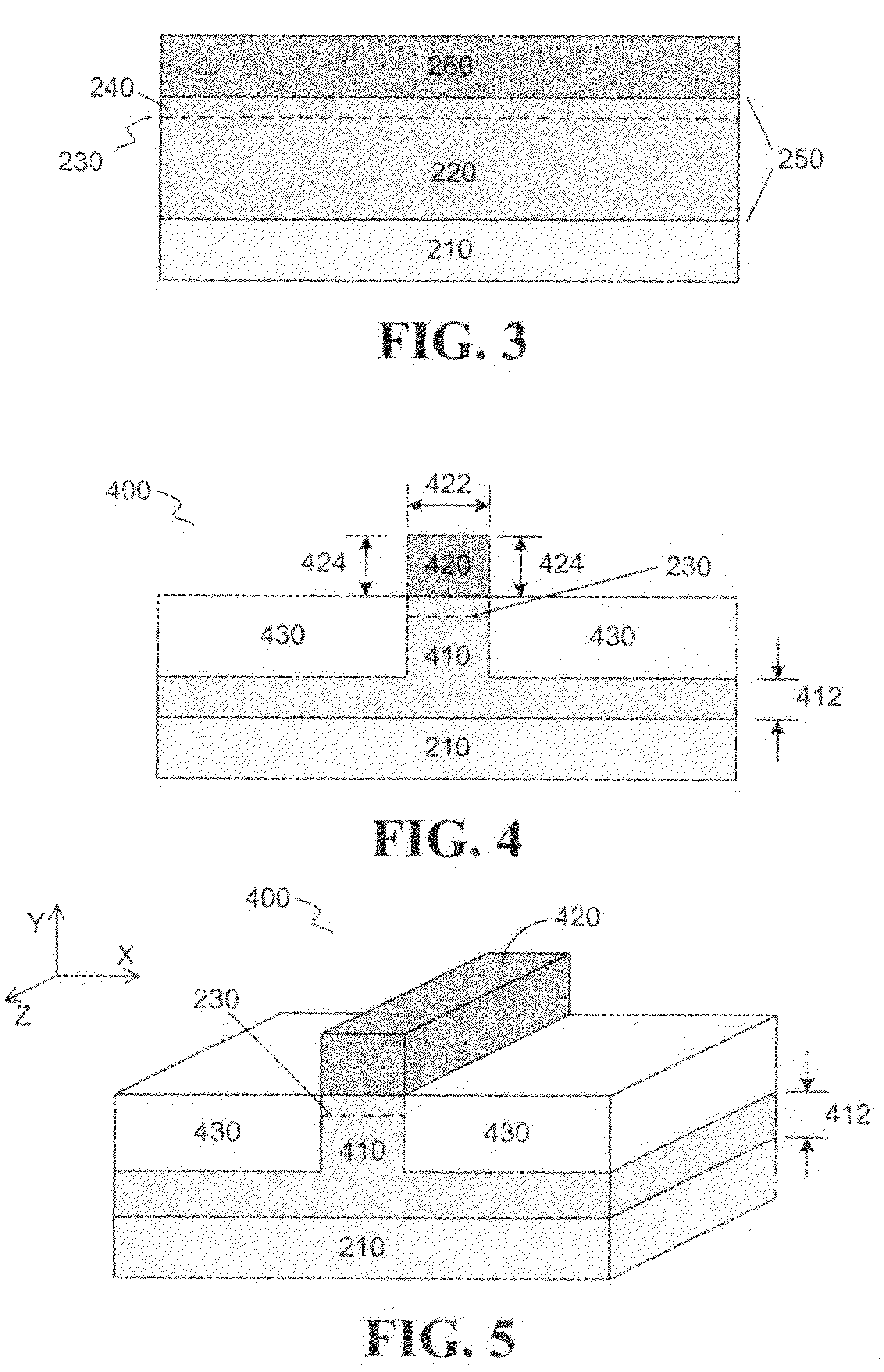
In various embodiments, an apparatus and methods for forming modulation doped non-planar transistors are described. In the following description, various embodiments will be described. However, one skilled in the relevant art will recognize that the various embodiments may be practiced without one or more of the specific details, or with other replacement and / or additional methods, materials, or components. In other instances, well-known structures, materials, or operations are not shown or described in detail to avoid obscuring aspects of various embodiments of the invention. Similarly, for purposes of explanation, specific numbers, materials, and configurations are set forth in order to provide a thorough understanding of the invention. Nevertheless, the invention may be practiced without specific details. Furthermore, it is understood that the various embodiments shown in the figures are illustrative representations and are not necessarily drawn to scale.

Reference throughout this...


PUM

PropertyMeasurementUnit
thicknessaaaaaaaaaa
thicknessaaaaaaaaaa
thicknessaaaaaaaaaa

Abstract

Embodiments of an apparatus and methods for providing three-dimensional complementary metal oxide semiconductor devices comprising modulation doped transistors are generally described herein. Other embodiments may be described and claimed.

Description

FIELD OF THE INVENTIONThe field of invention relates generally to the field of semiconductor integrated circuit manufacturing and, more specifically but not exclusively, relates to three-dimensional complementary metal oxide semiconductor (CMOS) devices comprising modulation doped transistors.BACKGROUND INFORMATIONA variety of electronic and optoelectronic devices can be enabled by developing thin film relaxed lattice constant III-V semiconductors on elemental silicon (Si) substrates. Surface layers capable of achieving the performance advantages of III-V materials may host a variety of high performance electronic devices such as complementary metal oxide semiconductor (CMOS) and modulation doped quantum well (QW) transistors fabricated from extreme high mobility materials such as, but not limited to, indium antimonide (InSb), indium gallium arsenide (InGaAs) and indium arsenide (InAs). Modulation doping is provided by doping a wide band gap semiconductor layer grown adjacent to a n...

Claims


Application Information

Patent Timeline
Patent Type & Authority Patents(United States)
IPC IPC(8): H01L29/778
CPCH01L29/66431H01L21/823892H01L21/823807H01L29/66462H01L29/0653H01L29/155H01L29/205H01L29/207H01L29/66795H01L29/7831
Inventor PILLARISETTY, RAVIHUDAIT, MANTURADOSAVLJEVIC, MARKORACHMADY, WILLYDEWEY, GILBERTKAVALIEROS, JACK
Owner INTEL CORP
Why Eureka
Try Eureka