Eureka AIR delivers breakthrough ideas for toughest innovation challenges, trusted by R&D personnel around the world.

Clustered field programmable gate array architecture

Active Publication Date: 2011-04-12
MICROSEMI SOC
View PDF37 Cites 8 Cited by
  • Summary
  • Abstract
  • Description
  • Claims
  • Application Information

AI Technical Summary

Problems solved by technology

Volatile control elements, such as SRAM bits, lose their programming data when the PLD power supply is disconnected, disabled or turned off.
Unfortunately, when such an approach is used in an FPGA cluster, the resulting performance degradation is undesirable to the point of being unacceptable in commercial FPGAs.
As the number of series switches increases, both the resistance and capacitance also increase which greatly increases the propagation delay through the network.
Adding buffers can help, but often the propagation delay through the buffers offsets the decrease in RC delays.

Method used


Image

  • Clustered field programmable gate array architecture
  • Clustered field programmable gate array architecture
  • Clustered field programmable gate array architecture

Examples


Embodiment Construction

[0056]Persons of ordinary skill in the art will realize that the following description of the present invention is illustrative only and not in any way limiting. Other embodiments of the invention will readily suggest themselves to such skilled persons.

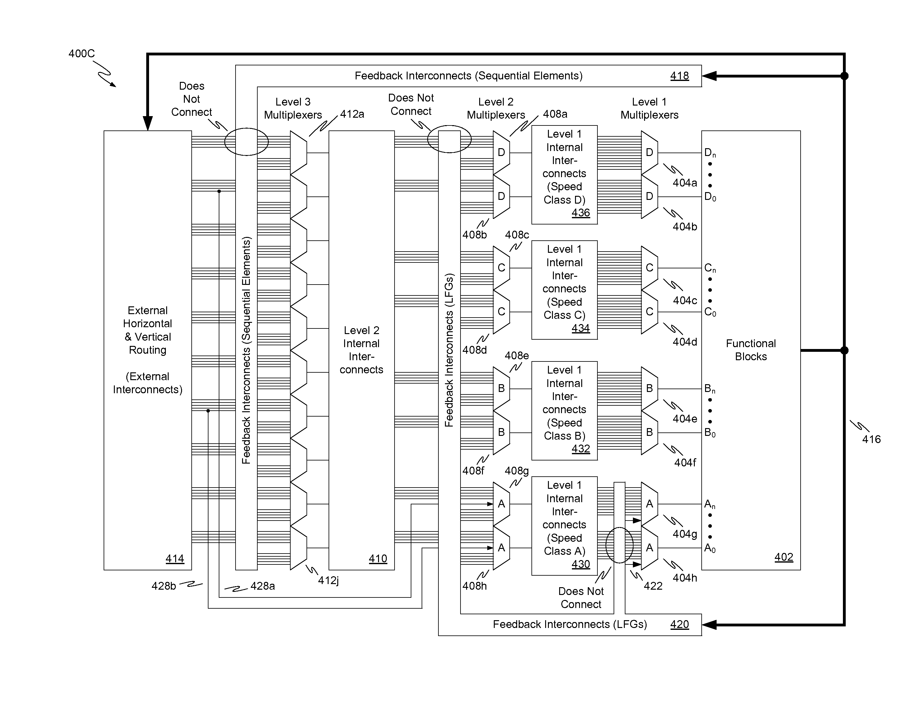
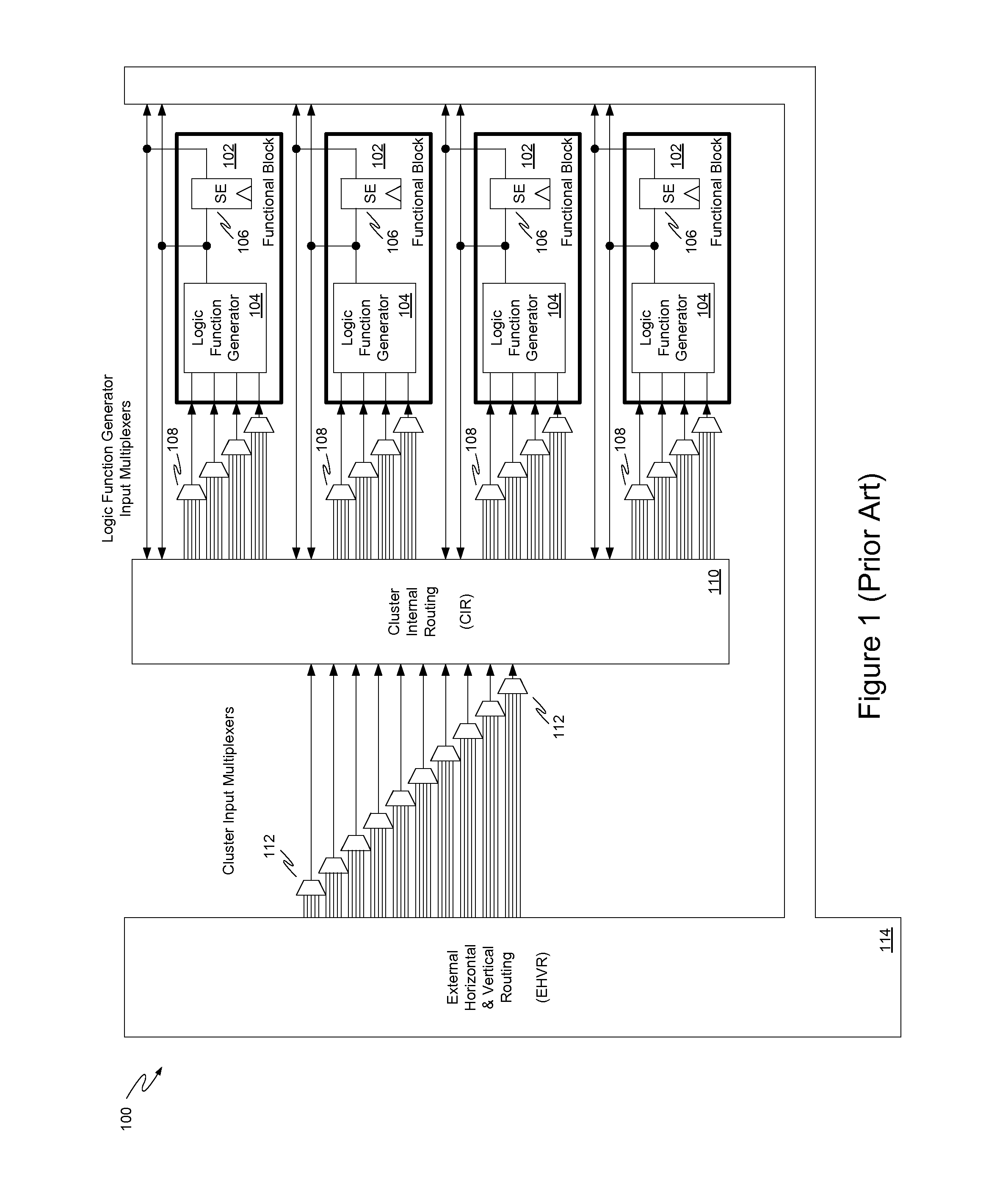
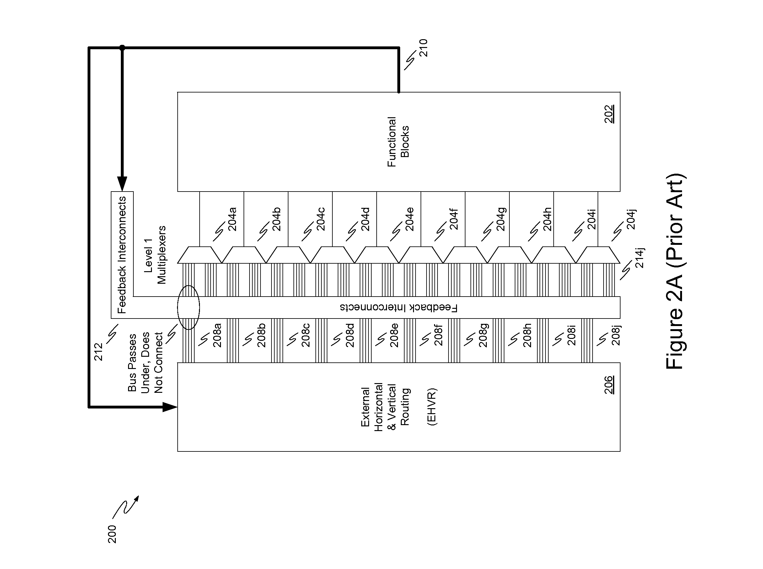
[0057]The present invention is a three level logic cluster which is organized in a manner that overcomes the performance limitations of the prior art. In comparison to the unacceptably slow I3F3 architecture shown in FIG. 2C the present invention has commercially acceptable performance while maintaining substantially the same area and routeability.

[0058]In the descriptions in this specification for the purpose of consistency and clarity of explanation only, the functional blocks in the logic cluster are assumed to include a mixture of LFGs (implemented as four input lookup tables or LUT4s) and sequential elements. In a preferred embodiment, an equal number of LUT4S and sequential elements are present, but this is not true in all embod...


PUM


Abstract

A logic cluster for a field programmable gate array integrated circuit device is disclosed. The cluster comprises a plurality of functional blocks and three levels of routing multiplexers. External signals enter the logic cluster primarily at the third level multiplexers with a few signals entering at the second level. Combinational outputs are fed back into the first and second level multiplexers while sequential outputs are fed back into the third level multiplexers. The logic function generators have permutable inputs with varying propagation delays. Routing signals between the first and second level multiplexers are grouped into speed classes and coupled to first level multiplexers associated with different logic function generators according to their speed class. Second and third level multiplexers are organized into groups such that routing signals between the second and third level multiplexers can be localized within the area occupied by the group. Groups are pitch matched to logic function generators to optimize and modularize area. Provision is made for global and local control of the sequential elements.

Description

REFERENCE TO RELATED APPLICATIONS[0001]This application claims an invention that was disclosed in Provisional Application No. 61 / 024,867 filed Jan. 30, 2008, entitled “Clustered Field Programmable Gate Array Architecture.” The benefit under 35 USC §119(e) of the United States provisional application is hereby claimed, and the aforementioned provisional application is hereby incorporated herein by reference.BACKGROUND OF THE INVENTION[0002]1. Field of the Invention[0003]The invention pertains to the field of integrated circuits. More particularly, the invention pertains to field programmable gate array integrated circuit devices.[0004]2. The Prior Art[0005]Field Programmable Gate Array (FPGA) integrated circuit devices are known in the art. An FPGA comprises any number of initially uncommitted functional blocks arranged in an array along with an appropriate amount of initially uncommitted routing resources. Functional blocks are circuits which can be configured to perform a variety o...

Claims


Application Information

Patent Timeline
IPC IPC(8): H01L25/00
CPCH03K19/177
Inventor KAPTANOGLU, SINANFENG, WENYI
Owner MICROSEMI SOC
Why Eureka
Eureka Blog
Learn More