Integrated circuit packaging system with multi-tier conductive interconnects and method of manufacture thereof

a technology of integrated circuit packaging and conductive interconnects, which is applied in the direction of electrical apparatus, semiconductor devices, semiconductor/solid-state device details, etc., can solve the problems of high cost, reliability challenges of pop designs, and long elude the skilled in the art, and achieve the effect of improving reliability and cos

Active Publication Date: 2011-04-19
STATS CHIPPAC LTD
View PDF12 Cites 97 Cited by
  • Summary
  • Abstract
  • Description
  • Claims
  • Application Information

AI Technical Summary

Problems solved by technology

POP designs face reliability challenges and higher cost.
Solutions to these problems have been long sought but prior develop...

Method used


Image

  • Integrated circuit packaging system with multi-tier conductive interconnects and method of manufacture thereof
  • Integrated circuit packaging system with multi-tier conductive interconnects and method of manufacture thereof
  • Integrated circuit packaging system with multi-tier conductive interconnects and method of manufacture thereof

Examples


first embodiment

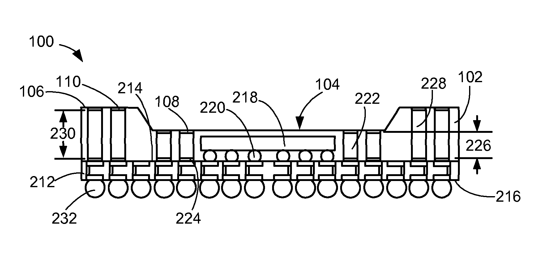
[0031]Referring now to FIG. 1, therein is shown a top view of an integrated circuit packaging system 100 in the present invention. The top view depicts an encapsulation 102, such as a cover including an epoxy molding compound or a wire in film. The encapsulation 102 can include an encapsulation recess 104 and an encapsulation plateau 106. The encapsulation recess 104 can be an inner portion of the encapsulation 102. The encapsulation plateau 106 can be along a peripheral portion of the encapsulation 102. As an example, the encapsulation plateau 106 is shown surrounding the encapsulation recess 104.

[0032]First contact pads 108 can be exposed from the encapsulation recess 104. The first contact pads 108 can be along an outer portion of the encapsulation recess 104. Second contact pads 110 can be exposed from the encapsulation plateau 106.

[0033]For illustrative purposes, the integrated circuit packaging system 100 is shown having the first contact pads 108 in a dual row configuration, ...

second embodiment

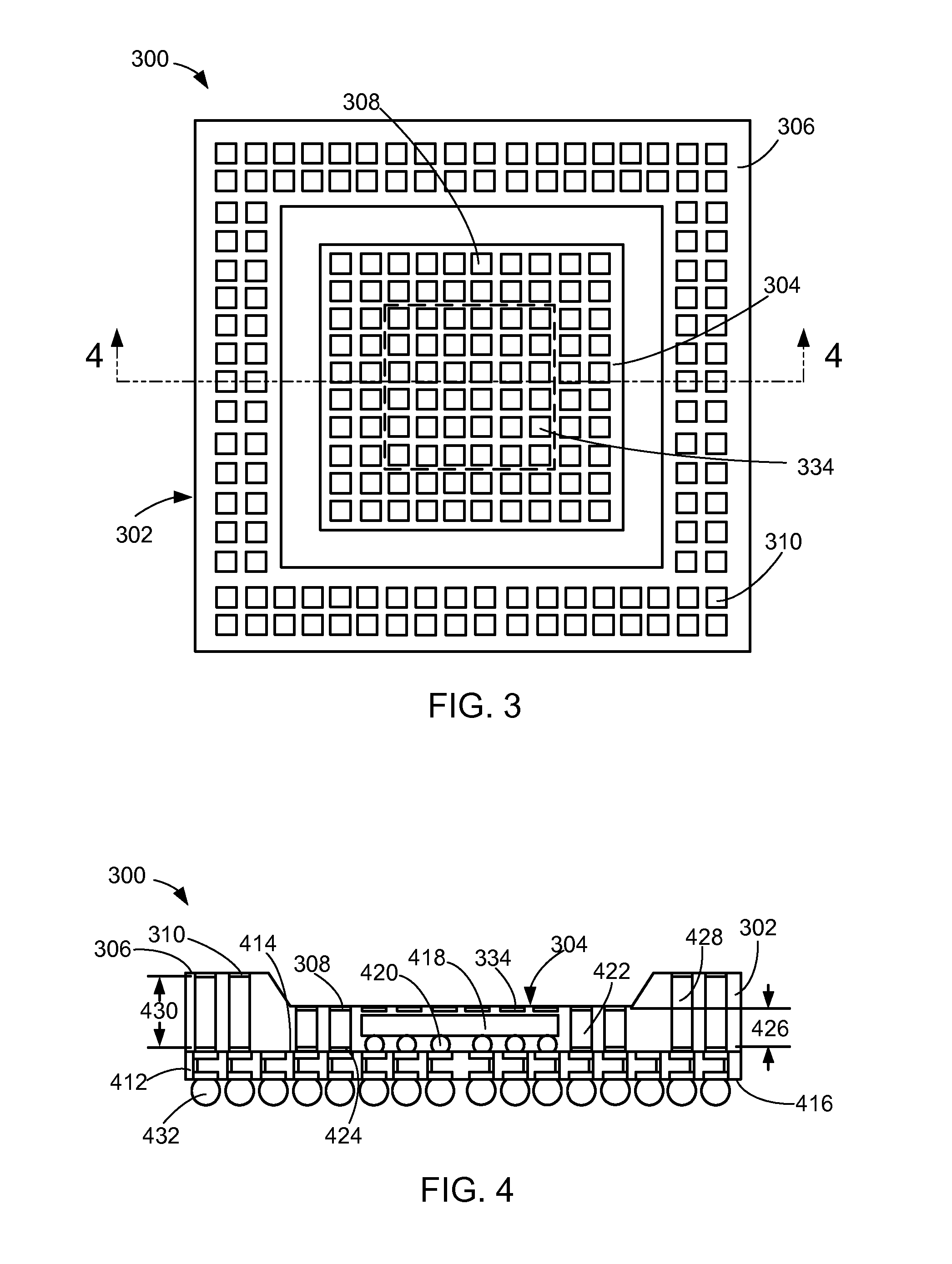
[0042]Referring now to FIG. 3, therein is shown a top view of an integrated circuit packaging system 300 in the present invention. The top view depicts an encapsulation 302, such as a cover including an epoxy molding compound a wire in film. The encapsulation 302 can include an encapsulation recess 304 and an encapsulation plateau 306. The encapsulation recess 304 can be an inner portion of the encapsulation 302. The encapsulation plateau 306 can be along a peripheral portion of the encapsulation 302. As an example, the encapsulation plateau 306 is shown surrounding the encapsulation recess 304.

[0043]Mounting pads 334, such as fan-in routed terminal pads, can be exposed from the encapsulation 302. The mounting pads 334 can be along the inner portion of the encapsulation recess 304, as depicted by the area surrounded by the dashed square.

[0044]For illustrative purposes, the integrated circuit packaging system 300 is shown having the mounting pads 334 in a grid configuration, although...

third embodiment

[0055]Referring now to FIG. 5, therein is shown a top view of an integrated circuit packaging system 500 in the present invention. The top view depicts an encapsulation 502, such as a cover including an epoxy molding compound a wire in film. The encapsulation 502 can include an encapsulation recess 504 and an encapsulation plateau 506. The encapsulation recess 504 can be an inner portion of the encapsulation 502. The encapsulation plateau 506 can be along a peripheral portion of the encapsulation 502. As an example, the encapsulation plateau 506 is sown surrounding the encapsulation recess 504. A conductive shield 540, such as a conductive sheet or coating, can be exposed from an inner portion of the encapsulation recess 504. The conductive shield 540 can be made from conductive materials including aluminum, nickel / silver, silver / gold alloys.

[0056]For illustrative purposes, the integrated circuit packaging system 500 is shown with the conductive shield 540 having a square shape,...


PUM


Abstract

A method of manufacture of an integrated circuit packaging system includes: providing a carrier having a planar surface and a cavity therein, a first barrier between the planar surface and a first interconnect, and a second barrier between the cavity and a second interconnect; providing a substrate; mounting an integrated circuit over the substrate; mounting the carrier to the substrate with the first interconnect and the second interconnect attached to the substrate and with the planar surface over the integrated circuit; forming an encapsulation between the substrate and the carrier covering the integrated circuit, the encapsulation having an encapsulation recess under the planar surface and over the integrated circuit; and removing a portion of the carrier to expose the encapsulation, a portion of the first barrier to form a first contact pad, and a portion of the second barrier to form a second contact pad.

Description

CROSS-REFERENCE TO RELATED APPLICATION[0001]The present application contains subject matter related to a concurrently filed U.S. Patent Application by NamJu Cho, HeeJo Chi, and HanGil Shin entitled “Carrier System with Multi-tier Conductive Posts and Method of Manufacture Thereof”. The related application is assigned to STATS ChipPAC Ltd. and is identified by Ser. No. 12 / 722,852. The subject matter thereof is incorporated herein by reference thereto.TECHNICAL FIELD[0002]The present invention relates generally to an integrated circuit packaging system, and more particularly to a system for an integrated circuit packaging system with multi-tier conductive interconnects.BACKGROUND ART[0003]Increased miniaturization of components, greater packaging density of integrated circuits (“ICs”), higher performance, and lower cost are ongoing goals of the computer industry. Semiconductor package structures continue to advance toward miniaturization, to increase the density of the components that...

Claims


Application Information

Patent Timeline
IPC IPC(8): H01L23/522
CPCH01L21/565H01L23/3128H01L23/49811H01L23/49827H01L23/552H01L25/105H01L23/13H01L2225/1088H01L23/49816H01L23/49838H01L24/16H01L24/97H01L2224/16225H01L2224/16227H01L2224/16235H01L2224/16238H01L2224/97H01L2225/1023H01L2225/1041H01L2225/1058H01L2225/1076H01L2924/15311H01L2924/15331H01L2924/1815H01L2224/81H01L2924/00014H01L2924/14H01L2924/00H01L2224/0401
Inventor CHO, NAMJUCHI, HEEJOSHIN, HANGIL
Owner STATS CHIPPAC LTD
Why Eureka
Try Eureka