
Power amplifier bias circuit

a power amplifier and bias circuit technology, applied in the direction of amplifiers, amplifiers with semiconductor devices only, amplifiers, etc., can solve the problems of increasing temperature, difficult to enable gaas-hbt power amplifiers to exhibit satisfactory distortion characteristics during low or medium output operation, etc., to achieve low distortion characteristics

Active Publication Date: 2011-05-03
MURATA MFG CO LTD
View PDF17 Cites 13 Cited by
  • Summary
  • Abstract
  • Description
  • Claims
  • Application Information

AI Technical Summary

Benefits of technology

The present invention provides a power amplifier bias circuit that can adjust the idle current of the amplifier transistor in response to its collector voltage, in order to minimize distortion. The circuit includes a voltage drive bias circuit, a current drive bias circuit, and an idle current control circuit. The idle current control circuit adjusts the bias current input to the amplifier transistor based on its collector voltage, ensuring that the power amplifier operates with low distortion. This results in improved performance and reliability.

Problems solved by technology

This problem becomes more acute with decrease in temperature, since the barrier voltage, which is determined by the device material, increases as the temperature decreases.
The present inventor has intensively studied this problem, and found it difficult to enable a GaAs-HBT power amplifier to exhibit satisfactory distortion characteristics during its low or medium output operation if the collector voltage of the amplifier transistors is reduced with the idle current maintained at the same level.

Method used


Image

  • Power amplifier bias circuit
  • Power amplifier bias circuit
  • Power amplifier bias circuit

Examples


first embodiment

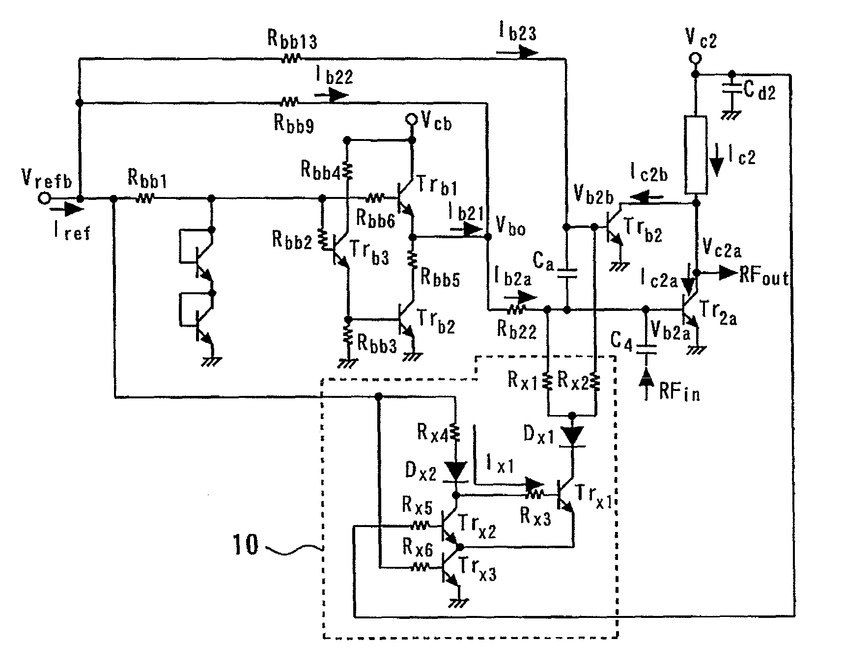
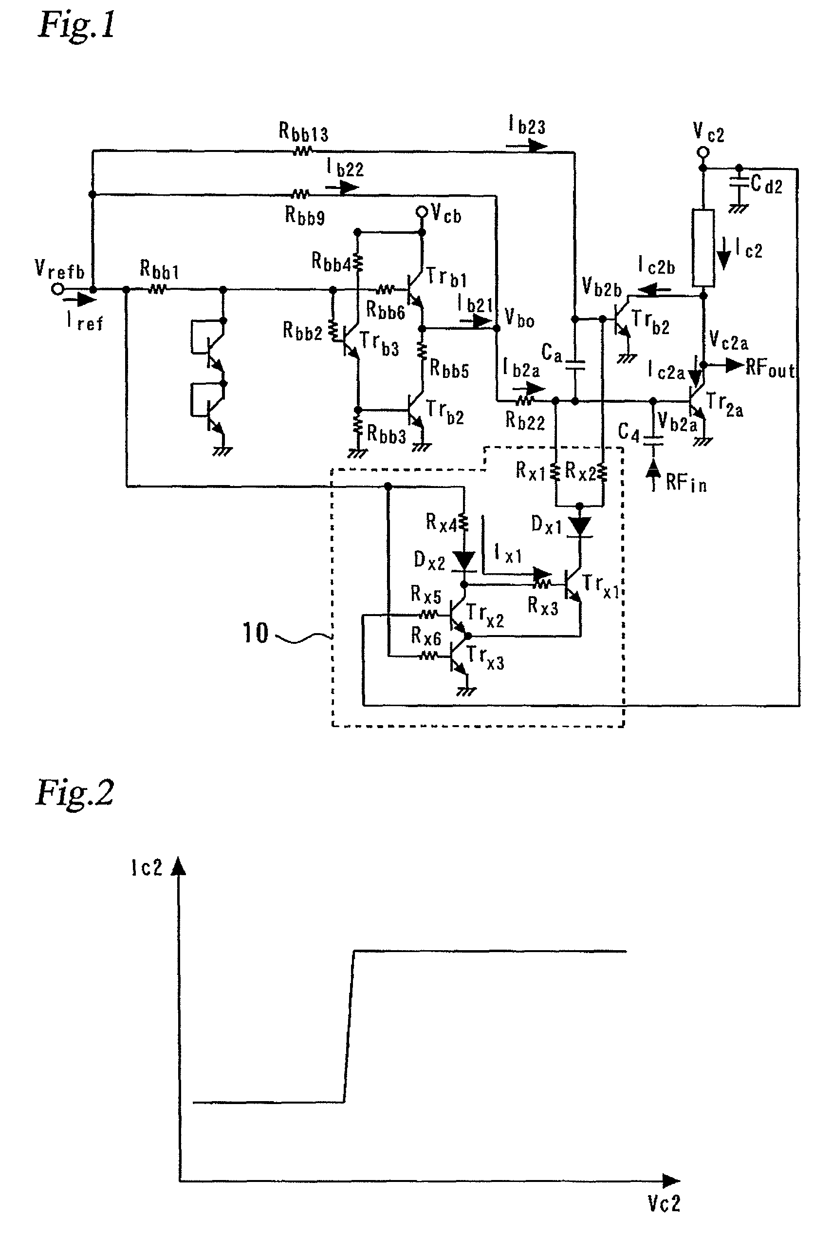
[0052]FIG. 1 is a circuit diagram showing a bias circuit for a GaAs-HBT power amplifier according to a first embodiment of the present invention. More specifically, FIG. 1 shows an exemplary configuration of a power amplifier and its bias circuit according to the first embodiment. This circuit uses GaAs-HBTs (Heterojunction Bipolar Transistors). In FIG. 1, those components common to the circuit diagrams shown in FIGS. 25 and 26 retain the same reference numerals and will not be described herein. Further, although the present embodiment will be described with reference to the second stage bias circuit of a two stage amplifier, it is to be understood that the embodiment may be applied to the first stage bias circuit, with the same effect.

[0053]The circuit configuration shown in FIG. 1 includes a voltage drive bias circuit and a current drive bias circuit connected in a parallel relationship to each other, wherein the voltage drive bias circuit typically includes an emitter follower an...

second embodiment

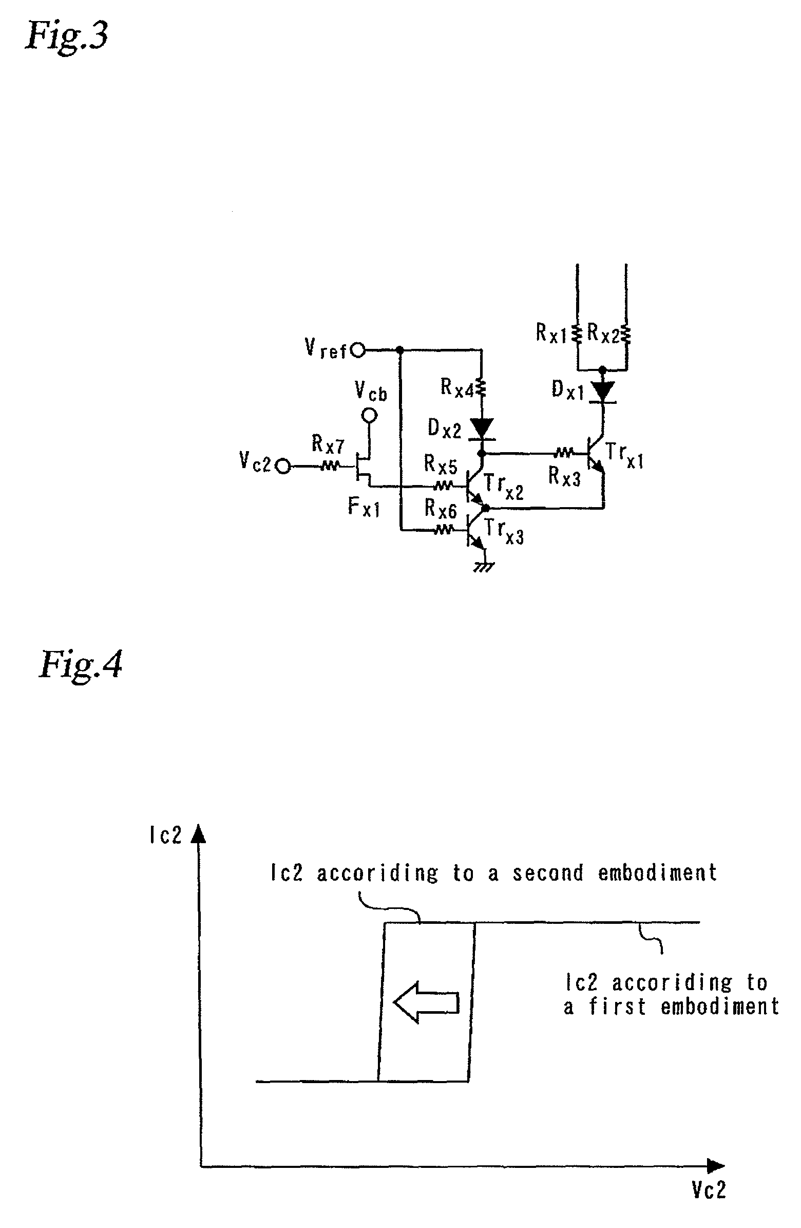
[0075]FIG. 3 is a circuit diagram showing the idle current control circuit of a GaAs-HBT power amplifier bias circuit according to a second embodiment of the present invention. Specifically, the circuit diagram shown in FIG. 3 is a part of a circuit diagram of the GaAs-HBT power amplifier bias circuit of the second embodiment, and illustrates the idle current control circuit 10 which uses the collector voltage Vc2 of the amplifier transistor. The power amplifier bias circuit of the second embodiment differs from that of the first embodiment in that the idle current control circuit 10 using the collector voltage Vc2 additionally includes an FET (Field Effect Transistor) connected to the Vc2 terminal side, which characterizes the second embodiment. The following description of the configuration of the second embodiment will focus on the differences from the first embodiment.

[0076]As shown in FIG. 3, the idle current control circuit 10 of the second embodiment includes a first FET (Fie...

third embodiment

[0079]FIG. 5 is a circuit diagram showing the idle current control circuit of a GaAs-HBT power amplifier bias circuit according to a third embodiment of the present invention. Specifically, the circuit diagram shown in FIG. 5 is a part of a circuit diagram of the GaAs-HBT power amplifier bias circuit of the third embodiment, and illustrates the idle current control circuit 10 which uses the collector voltage Vc2 of the amplifier transistor. The power amplifier bias circuit of the third embodiment differs from that of the second embodiment in that the idle current control circuit 10 using the collector voltage Vc2 additionally includes a Schottky barrier diode Dx3 connected to the Vc2 terminal side (see FIG. 5), which characterizes the third embodiment.

[0080]Specifically, in the third embodiment the Schottky barrier diode Dx3 is connected between the FET Fx1 and the resistance Rx5, as shown in FIG. 5. The anode of Dx3 is connected to the source of Fx1, and the cathode of Dx3 is conne...


PUM


Abstract

A power amplifier and bias circuit includes a combination circuit in which a voltage drive bias circuit and a current drive bias circuit are connected in a parallel relationship with each other. The power amplifier bias circuit also includes an idle current control circuit which uses the collector voltage of amplifier transistors. When the collector voltage of the amplifier transistors is lower than the threshold voltage of a first transistor (approximately 1.3 V), the first transistor is turned off. At that time, since the reference voltage (2.4-2.5 V) is higher than the voltage for turning on both a second transistor and a diode (namely, approximately 1.3 V plus 0.7 V), a current flows and the first transistor turns on. As a result, a current is drawn from the bases of the amplifier transistors to GND through two resistances, so that the idle currents of the amplifier transistors decrease.

Description

FIELD OF THE INVENTION[0001]The present invention relates to a power amplifier bias circuit, and more particularly to a power amplifier bias circuit for use in power amplifiers for mobile communications such as cellular phones.BACKGROUND ART[0002]GaAs-HBT (Heterojunction Bipolar Transistor) power amplifiers are currently widely used as cellular phone power amplifiers for CDMA (Code Division Multiple Access), etc. FIG. 25, which includes FIGS. 25A and 25B, shows an exemplary circuit of a GaAs-HBT power amplifier module. In FIG. 25A, the GaAs chip is represented by broken lines; the other circuit elements include chip components and transmission lines formed on the module substrate.[0003]Referring to the figure, symbol IN denotes an RF signal input terminal; OUT, an RF signal output terminal; Vc1, the collector power terminal for the first stage transistor; Vc2, the collector power terminal for the last stage transistor; Vcb, the power terminal for the bias circuits for the first and ...

Claims


Application Information

Patent Timeline
Patent Type & Authority Patents(United States)
IPC IPC(8): H03F3/04
CPCH03F1/0261H03F3/195H03F3/245H03F2200/555H03F2200/18H03F2200/451
Inventor MATSUZUKA, TAKAYUKIYAMAMOTO, KAZUYAOKAMURA, ATSUSHI
Owner MURATA MFG CO LTD
Learn More