

Semiconductor device having a fin field effect transistor
a technology of field effect transistor and semiconductor device, which is applied in the direction of semiconductor device, transistor, electrical apparatus, etc., can solve the problems of not easy to achieve the finfet of the related art, and achieve the effect of wide band, low distortion characteristic, and easy to achieve high gain
- Summary
- Abstract
- Description
- Claims
- Application Information
AI Technical Summary
Benefits of technology
Problems solved by technology
Method used
Image

Examples
first embodiment
(Structure)
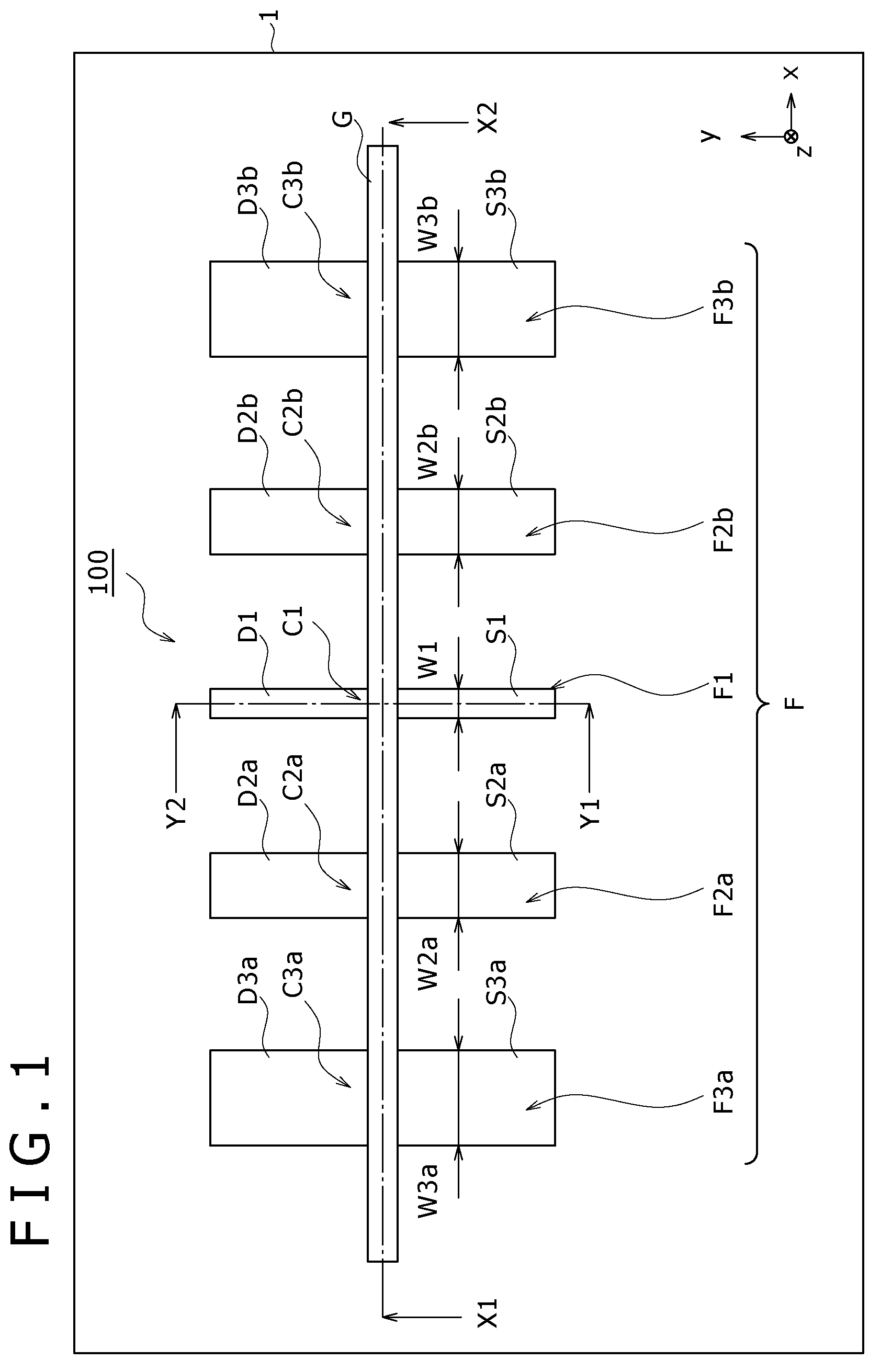
[0043]FIG. 1 is a plan view schematically showing major part of a semiconductor device according to a first embodiment of the present invention.
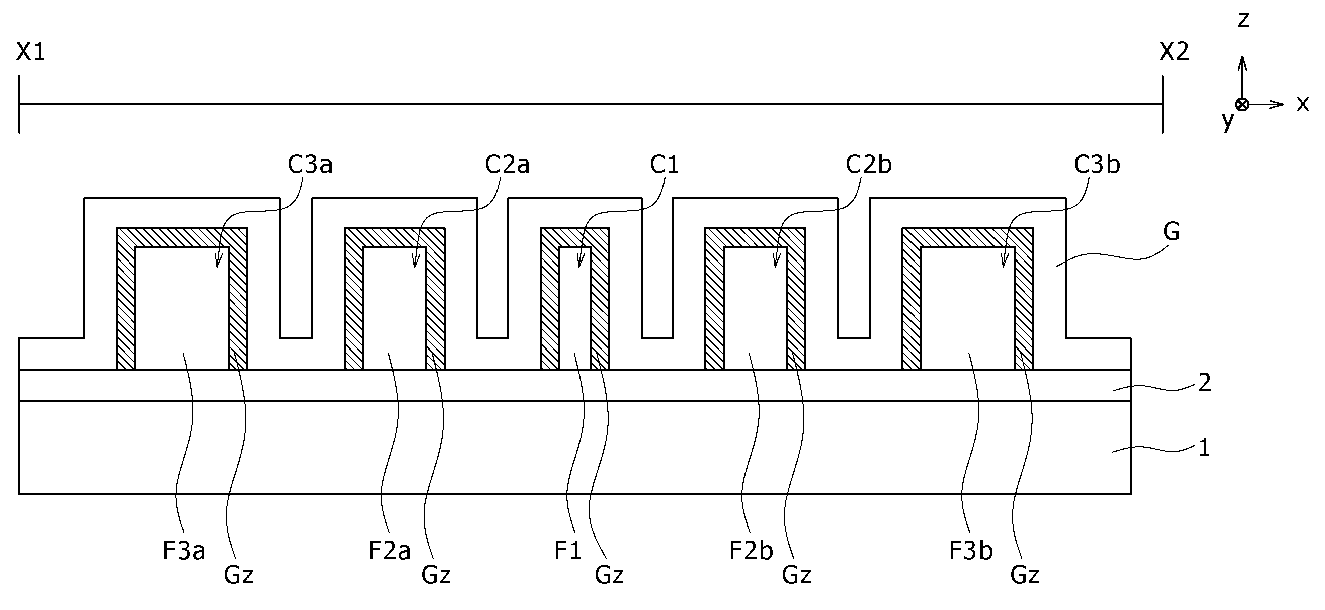
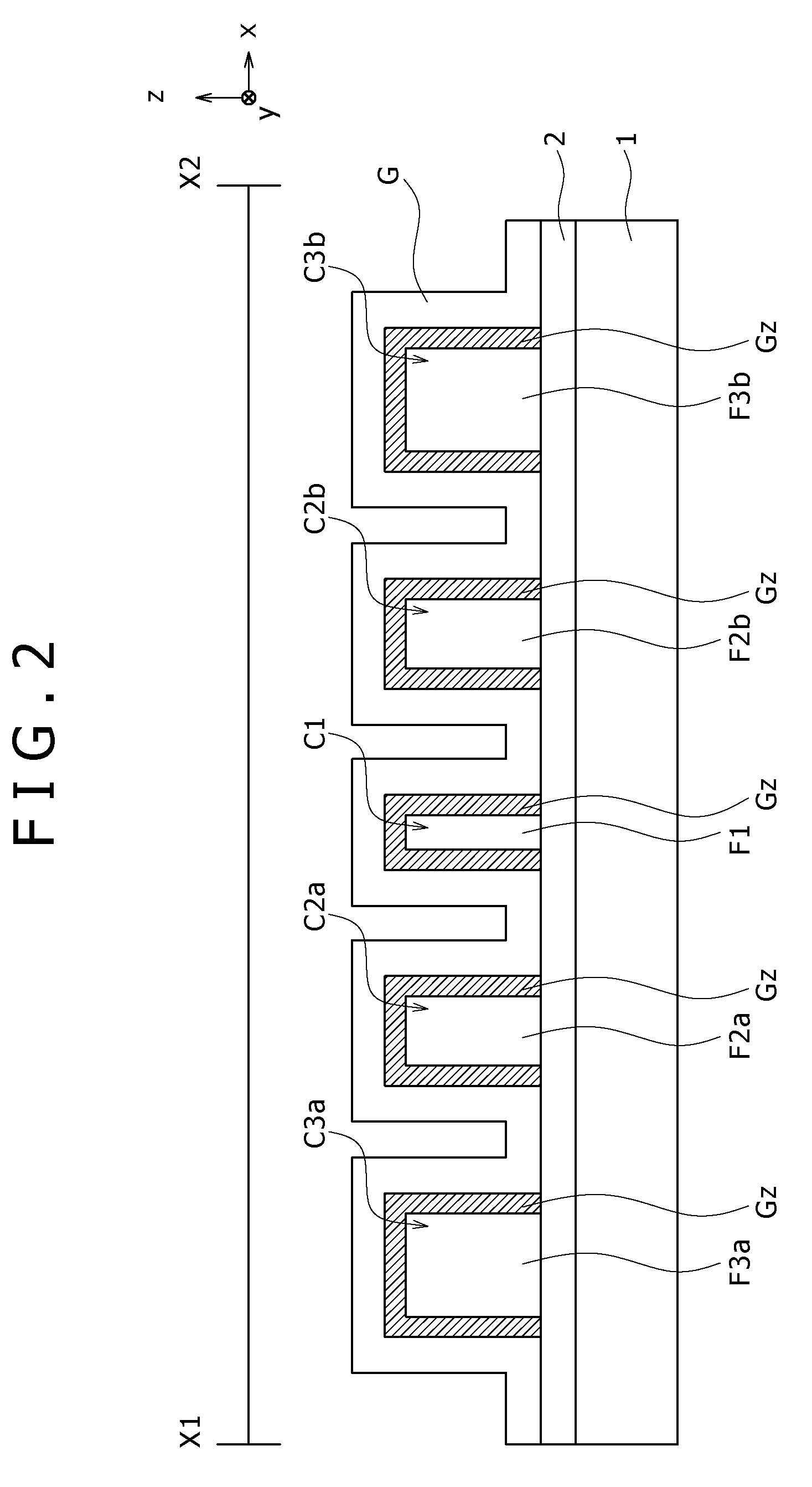
[0044]FIGS. 2 and 3 are sectional views schematically showing major part of the semiconductor device according to the first embodiment of the present invention.
[0045]Specifically, FIG. 2 is a sectional view corresponding to the plane that is along line X1-X2 in FIG. 1 and perpendicular to the paper plane of FIG. 1. FIG. 3 is a sectional view corresponding to the plane that is along line Y1-Y2 in FIG. 1 and perpendicular to the paper plane of FIG. 1.
[0046]As shown in FIG. 1, the semiconductor device of the present embodiment has a finFET 100. The finFET 100 includes fins F and a gate electrode G.
[0047]In this finFET 100, the fins F include five fins F1, F2a, F2b, F3a, and F3b as shown in FIG. 1. These five fins F1, F2a, F2b, F3a, and F3b are formed of e.g. a silicon semiconductor.
[0048]Each of five fins F1, F2a, F2b, F3a, and F3b o...
second embodiment
[0147]A second embodiment of the present invention will be described below.
(Structure)
[0148]FIG. 16 is a plan view showing major part of a semiconductor device according to the second embodiment of the present invention.
[0149]FIGS. 17 and 18 are sectional views schematically showing major part of the semiconductor device according to the second embodiment of the present invention.
[0150]Specifically, FIG. 17 is a sectional view corresponding to the plane that is along line X1-X2 in FIG. 16 and perpendicular to the paper plane of FIG. 16. FIG. 18 is a sectional view corresponding to the plane that is along line Y1-Y2 in FIG. 16 and perpendicular to the paper plane of FIG. 16.
[0151]The present embodiment is different from the first embodiment in the fins F included in the finFET 100 as shown in FIGS. 16 to 18. Except for this feature, the second embodiment is the same as the first embodiment. Therefore, the description of the overlapping part is omitted.
[0152]In the finFET 100 of the p...
third embodiment
[0199]A third embodiment of the present invention will be described below.
(Structure)
[0200]FIG. 22 is a plan view showing major part of a semiconductor device according to the third embodiment of the present invention.
[0201]FIGS. 23 and 24A to 24C are sectional views schematically showing major part of the semiconductor device according to the third embodiment of the present invention.
[0202]Specifically, FIG. 23 is a sectional view corresponding to the plane that is along line X1-X2 in FIG. 22 and perpendicular to the paper plane of FIG. 22. FIG. 24A is a sectional view corresponding to the plane that is along line Y1-Y2 in FIG. 22 and perpendicular to the paper plane of FIG. 22. FIG. 24B is a sectional view corresponding to the plane that is along line Y1b-Y2b in FIG. 22 and perpendicular to the paper plane of FIG. 22. FIG. 24C is a sectional view corresponding to the plane that is along line Y1c-Y2c in FIG. 22 and perpendicular to the paper plane of FIG. 22.
[0203]The present embod...
PUM
 Abstract
Description
Claims
Application Information