Method in the fabrication of a monolithically integrated high frequency circuit

a high frequency circuit and monolithic technology, applied in the direction of basic electric elements, electrical apparatus, semiconductor devices, etc., can solve the problems of inability to meet the requirements of an optimized drain drift region, the light doping well used for this purpose, and the normal use of standard processes, etc., to achieve convenient use, save chip area, and compact layout

Inactive Publication Date: 2005-05-26
INFINEON TECH AG
View PDF5 Cites 96 Cited by
  • Summary
  • Abstract
  • Description
  • Claims
  • Application Information

AI Technical Summary

Benefits of technology

[0027] Since the current path will be partially vertical along the wall of the shallow trench, a more compact layout will be achieved, which saves chip area.
[0028] The combination of the DMOS power transistor produced according to the present invention with other transistors easily achievable on a single chip and analog, mixed signal and RF BiCMOS devices leads to an attractive variety of circuit design options otherwise not easily available.

Problems solved by technology

The lightly doped wells used for this purpose and normally present in standard processes will not in a general case fulfill the requirements needed for an optimized drain drift region.
This is particularly accentuated in a technology using shallow trench isolation (STI), where the STI occupies a large portion of the well, which makes it almost impossible to use conventional wells.

Method used


Image

  • Method in the fabrication of a monolithically integrated high frequency circuit
  • Method in the fabrication of a monolithically integrated high frequency circuit
  • Method in the fabrication of a monolithically integrated high frequency circuit

Examples


Embodiment Construction

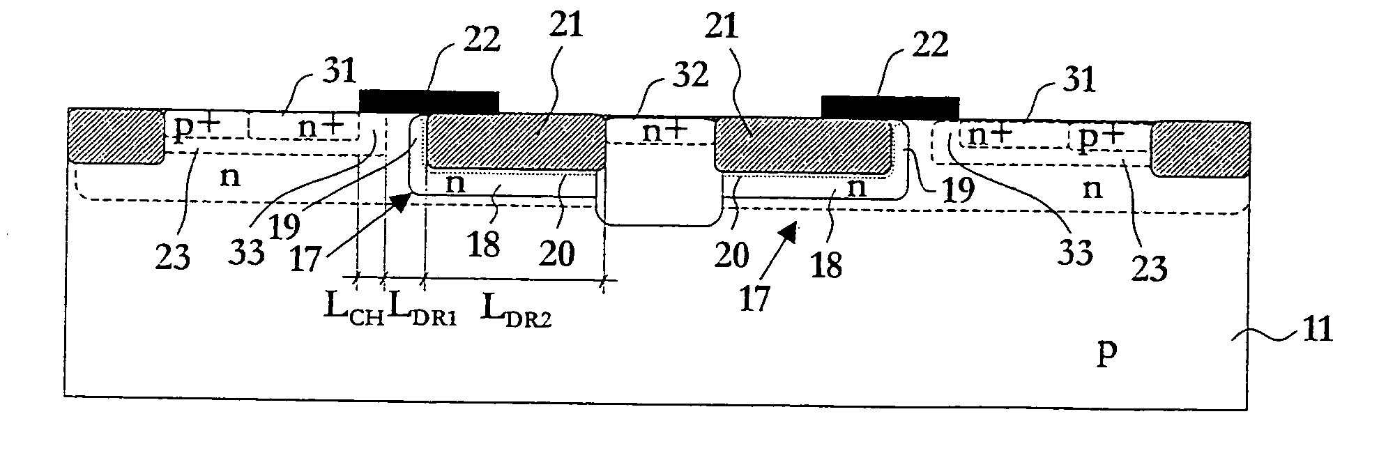
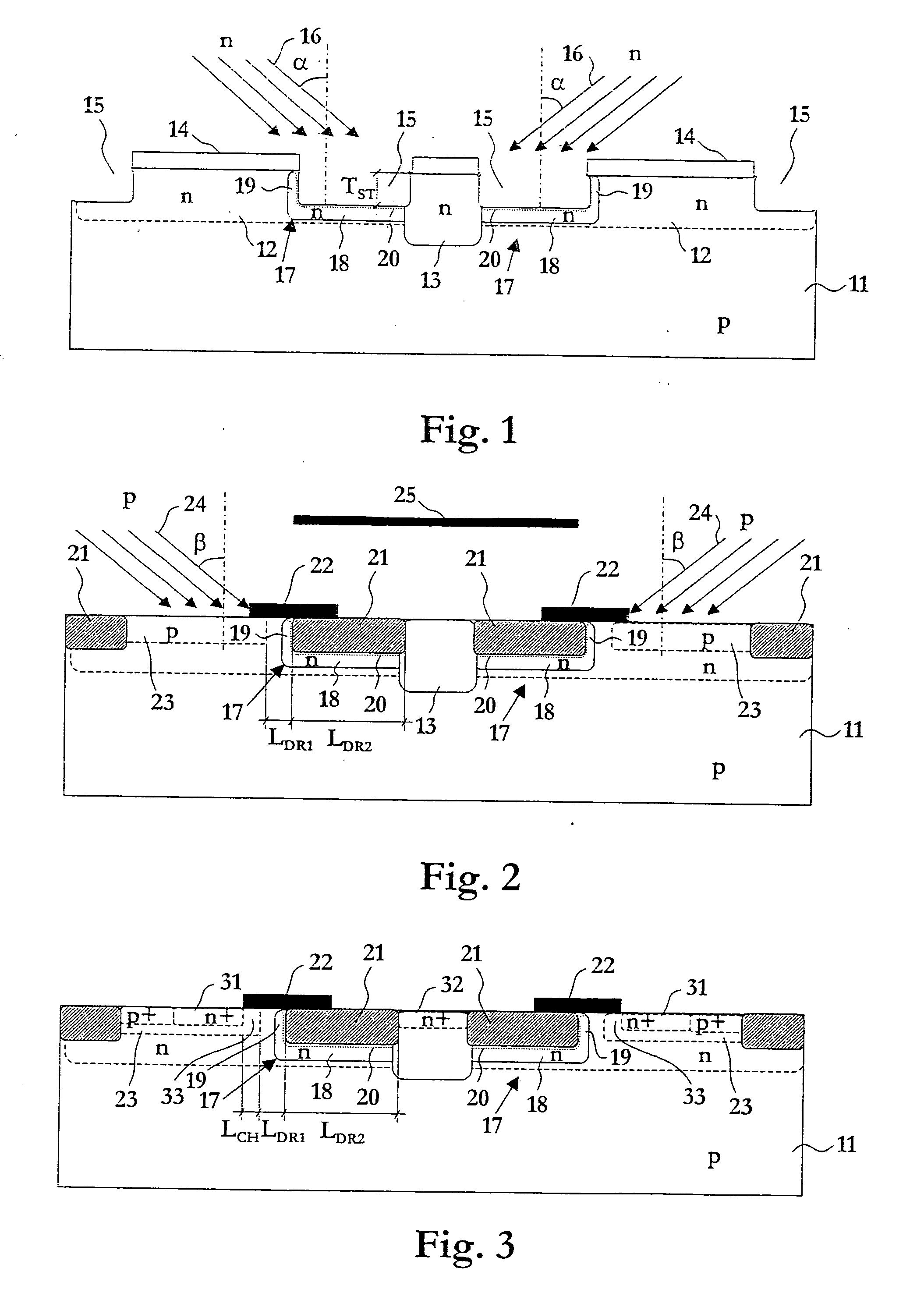
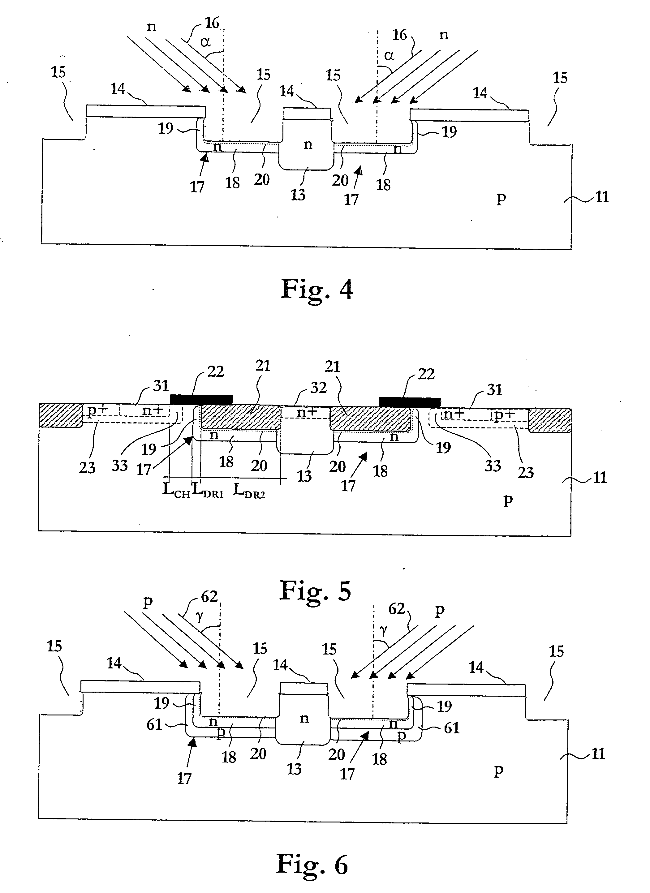
[0034] A first preferred embodiment of a method in the fabrication of a monolithically integrated circuit including a DMOS (double diffused MOS) transistor is described below with reference to FIGS. 1-3. The method is implemented in a BiCMOS process. Many of the process steps, e.g. including formation of a gate and ion implantation of wells and source and drain regions, are well known to the person skilled in the art and these steps will therefore not be described at all here, or will only be schematically indicated. The main focus is put on how the extended drain of the DMOS transistor is formed.

[0035] A semiconductor structure including a partially processed DMOS transistor is shown in FIG. 1 in a cross section. Reference numeral 11 denotes the p-type doped silicon substrate, 12 denotes an n-type doped well region typically used for bipolar transistors in the BiCMOS process, and 13 denotes an n-type doped well region typically used for MOS transistors in the BiCMOS process. An n+...


PUM


Abstract

A method in the fabrication of an integrated high frequency circuit including a DMOS transistor device comprises the steps of providing a substrate, etching a trench in a region defined for an extended drain for the DMOS transistor, and doping a region below the trench and a region at a side of the trench to a first doping type by means of ion implantation in the etched open trench through a mask, wherein the ion implantation is effectuated in a direction, which is inclined at an angle to the normal of the surface of the substrate, to thereby create a partly lateral and partly vertical current path in the extended drain. The method comprises further the steps of filling the trench with an insulating material to form a shallow trench isolation region, and forming a gate, a channel region, a source, and a drain for the DMOS transistor.

Description

PRIORITY [0001] This application claims priority to Swedish application no. 0303099-6 filed Nov. 21, 2003. TECHNICAL FIELD OF THE INVENTION [0002] The present invention generally relates to the field of integrated circuit technology, and more specifically the invention relates to a method in the fabrication of a monolithically integrated circuit, to a DMOS transistor device, and to a monolithically integrated circuit, respectively. DESCRIPTION OF RELATED ART AND BACKGROUND OF THE INVENTION [0003] The ever-increasing market for microwave power amplifiers in PCS, CDMA, and WCDMA systems requires low cost, and ease of use technology that can provide high power and good linearity performance. LDMOS devices started to replace bipolar devices in base station applications 3-4 years ago and LDMOS has for multiple reasons become the leading technology for base station power amplifier applications. The LDMOS device has high gain and shows excellent back-off linearity. The breakdown voltage BV...

Claims


Application Information

Patent Timeline
Patent Type & Authority Applications(United States)
IPC IPC(8): H01LH01L21/265H01L21/336H01L29/06H01L29/08H01L29/10H01L29/78
CPCH01L21/26586H01L29/0653H01L29/0878H01L29/7835H01L29/66659H01L29/66681H01L29/7816H01L29/1083H01L29/063H01L29/1045
Inventor LITWIN, ANDREJ
Owner INFINEON TECH AG
Why Eureka
Try Eureka