
Error-detecting and correcting FPGA architecture

a technology of error detection and error correction, applied in the field of fpga integrated circuits, can solve the problems of no way to detect failures, and the change in the contents of configuration memory is likely to have disastrous consequences for the circuit implemented in the fpga integrated circui

Active Publication Date: 2011-05-03
MICROSEMI SOC
View PDF21 Cites 14 Cited by
  • Summary
  • Abstract
  • Description
  • Claims
  • Application Information

AI Technical Summary

Benefits of technology

The present invention relates to a method for programming an FPGA integrated circuit with a non-volatile memory. The method includes generating ECC data from the FPGA configuration data and writing the ECC data into a separate memory cell. The method also includes checking the integrity of the memory bits during boot-up and reprogramming any errors detected. The technical effect of this invention is to provide a reliable and efficient method for programming FPGAs with non-volatile memory.

Problems solved by technology

Whenever the state of a single memory cell in a non-volatile-memory-based FPGA changes due to ionizing radiation or for any other reason, there is presently no way to detect the failure.
Because the FPGA configuration depends on the programmed or unprogrammed status of the non-volatile memory cells, any change in the contents of the configuration memory is likely to have disastrous consequences for the circuit implemented in the FPGA integrated circuit.

Method used


Image

  • Error-detecting and correcting FPGA architecture
  • Error-detecting and correcting FPGA architecture
  • Error-detecting and correcting FPGA architecture

Examples


Embodiment Construction

[0011]Persons of ordinary skill in the art will realize that the following description of the present invention is illustrative only and not in any way limiting. Other embodiments of the invention will readily suggest themselves to such skilled persons.

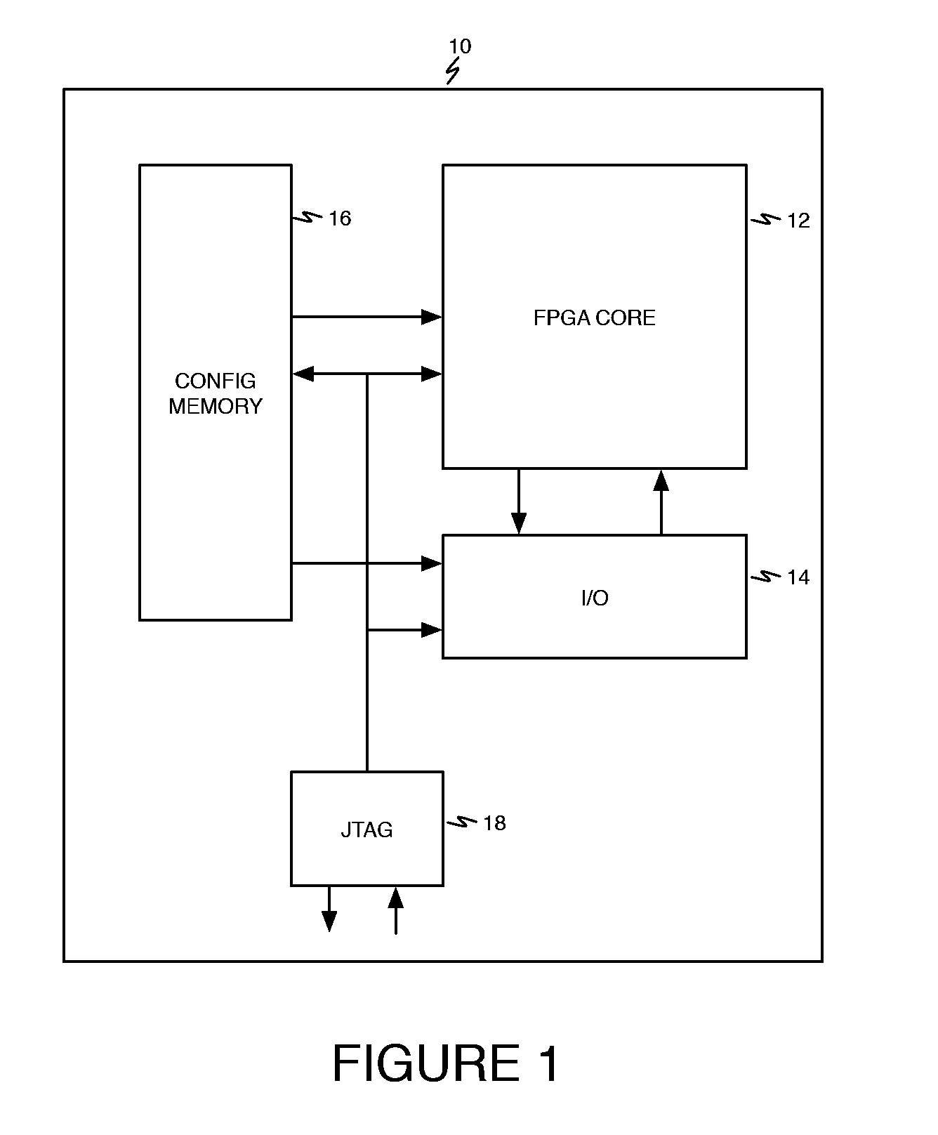
[0012]Referring first to FIG. 1, a simplified block diagram shows an illustrative non-volatile memory based FPGA integrated circuit 10 according to the present invention. Persons of ordinary skill in the art will appreciate that FPGA 10 may also include additional circuit blocks, such as user memory and other circuit blocks that are not shown in FIG. 1.

[0013]As is known in the art, FPGA 10 includes and FPGA core 12 that includes a plurality of programmable circuit elements and programmable interconnect elements that are used to configure the user circuit. FPGA core 12 is coupled to input / output (I / O) block 14. I / O block 14 includes a plurality of I / O circuits that can be programmably connected to the circuit elements in the FPGA core ...


PUM


Abstract

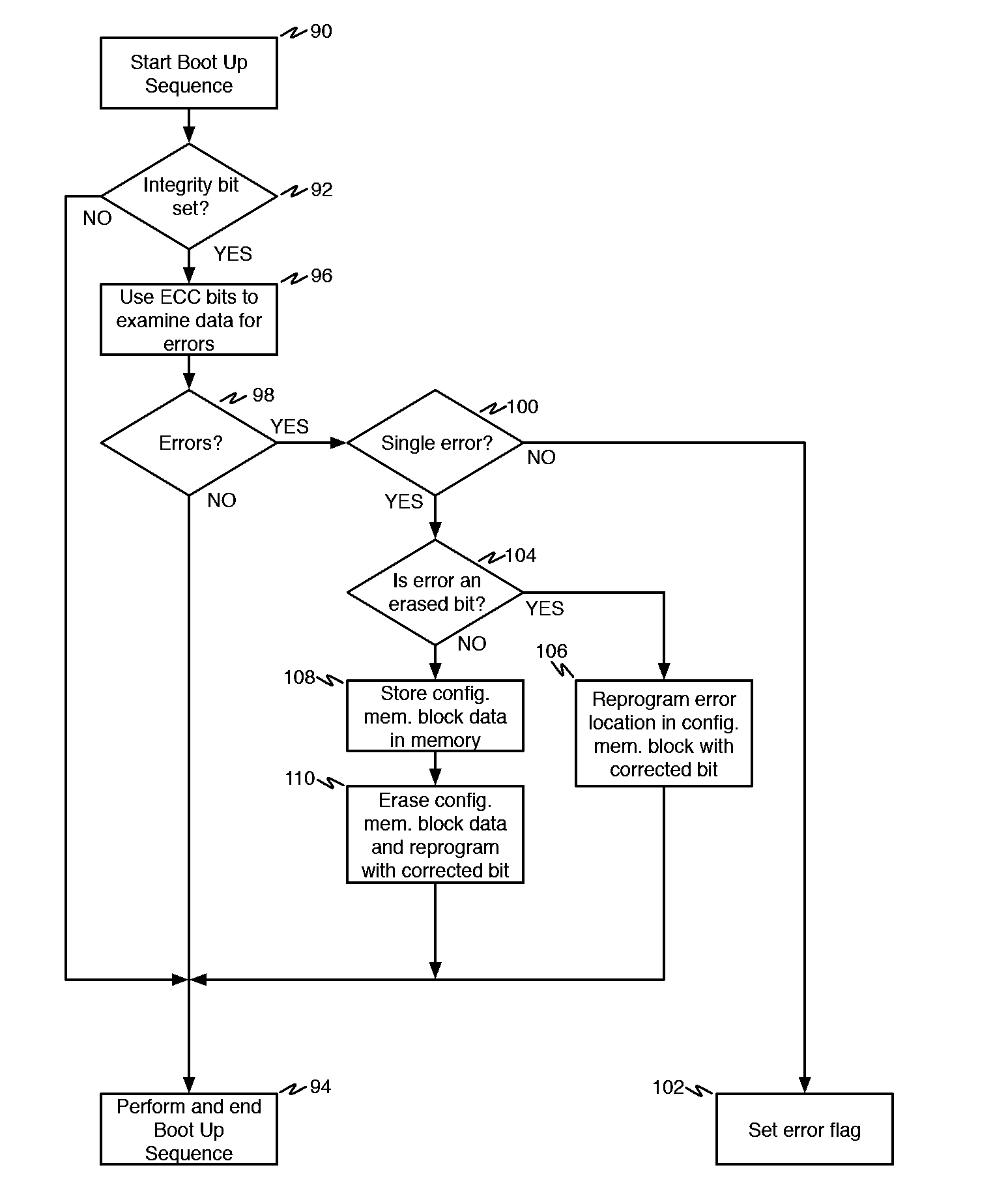
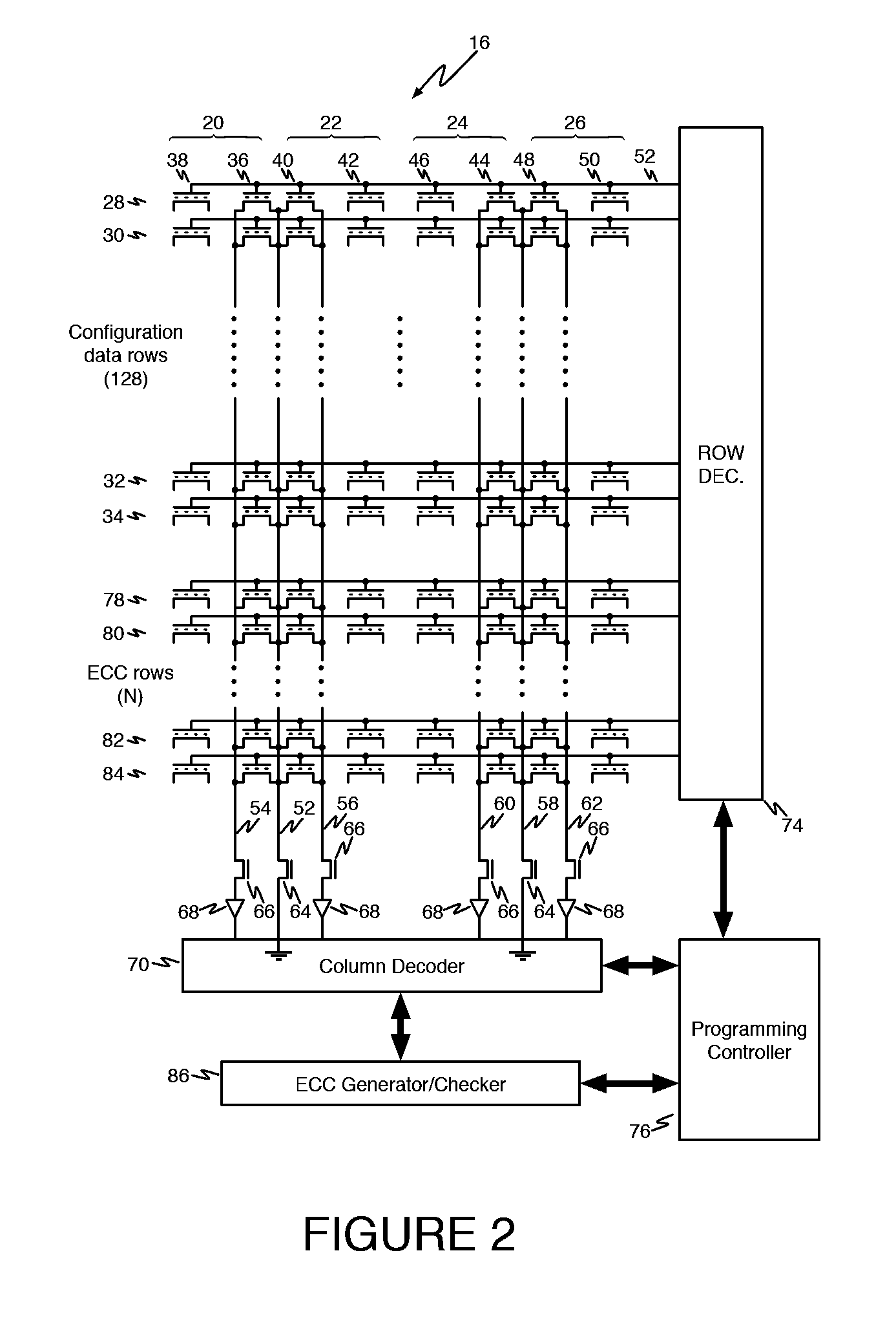
A method and apparatus are provided for an error-correcting FPGA. ECC data for configuration is generated and programmed into the ECC rows in the configuration memory. While booting, it is determined whether an integrity-check bit is set. If so, an integrity check is performed. If a single-bit error is detected, if the bit error is an erroneous “0” value, the memory location containing the erroneous “0” value is reprogrammed to a “1” value. If the bit error is an erroneous “1,” value, the memory block data is saved in a non-volatile memory block, the configuration memory block containing the error is erased and reprogrammed using the corrected bit. If there is more than one error, an error flag is set. The user reads the status of the error flag through the JTAG port. If the error flag is set then a full reprogramming cycle is initiated.

Description

BACKGROUND OF THE INVENTION[0001]1. Field of the Invention[0002]The present invention relates to programmable logic devices such as field-programmable gate array (FPGA) integrated circuits. More particularly, the present invention relates to FPGA integrated circuits using non-volatile memory for providing configuration information for the FPGA and to a non-volatile FPGA configuration memory with an ECC generator / checker for generating ECC information and memory cells reserved for storage of ECC information generated by the ECC generator / checker.[0003]2. The Prior Art[0004]An FPGA includes programmable circuitry that is configured and interconnected using programmable elements. Some FPGA integrated circuits employ non-volatile memory cells, such as flash memory cells, as the programmable elements. Whenever the state of a single memory cell in a non-volatile-memory-based FPGA changes due to ionizing radiation or for any other reason, there is presently no way to detect the failure. Be...

Claims


Application Information

Patent Timeline
Patent Type & Authority Patents(United States)
IPC IPC(8): G11C29/00H03M13/00
CPCG06F11/1052H03K19/17764H03K19/1776G11C2029/0411
Inventor BELLIPADDY, VIDYADHARABAKKER, GREGORY
Owner MICROSEMI SOC
Learn More