
FPGA architecture having two-level cluster input interconnect scheme without bandwidth limitation

a technology of fpga architecture and cluster input, which is applied in the direction of instruments, computation using denominational number representation, pulse technique, etc., can solve the problems of bandwidth limitation, bandwidth limitation is the number, and the bandwidth limitation of prior-art two-level schemes, so as to improve connectivity and the effect of routing structur

Active Publication Date: 2008-08-05
MICROSEMI SOC
View PDF2 Cites 7 Cited by
  • Summary
  • Abstract
  • Description
  • Claims
  • Application Information

AI Technical Summary

Benefits of technology

[0018]In the prior art, the Monte Carlo method is used for measuring routability. This method picks a large number of random routing vectors, and measures the percentage of them that can be routed on a routing structur...

Problems solved by technology

Prior-art two-level schemes have bandwidth limitations.
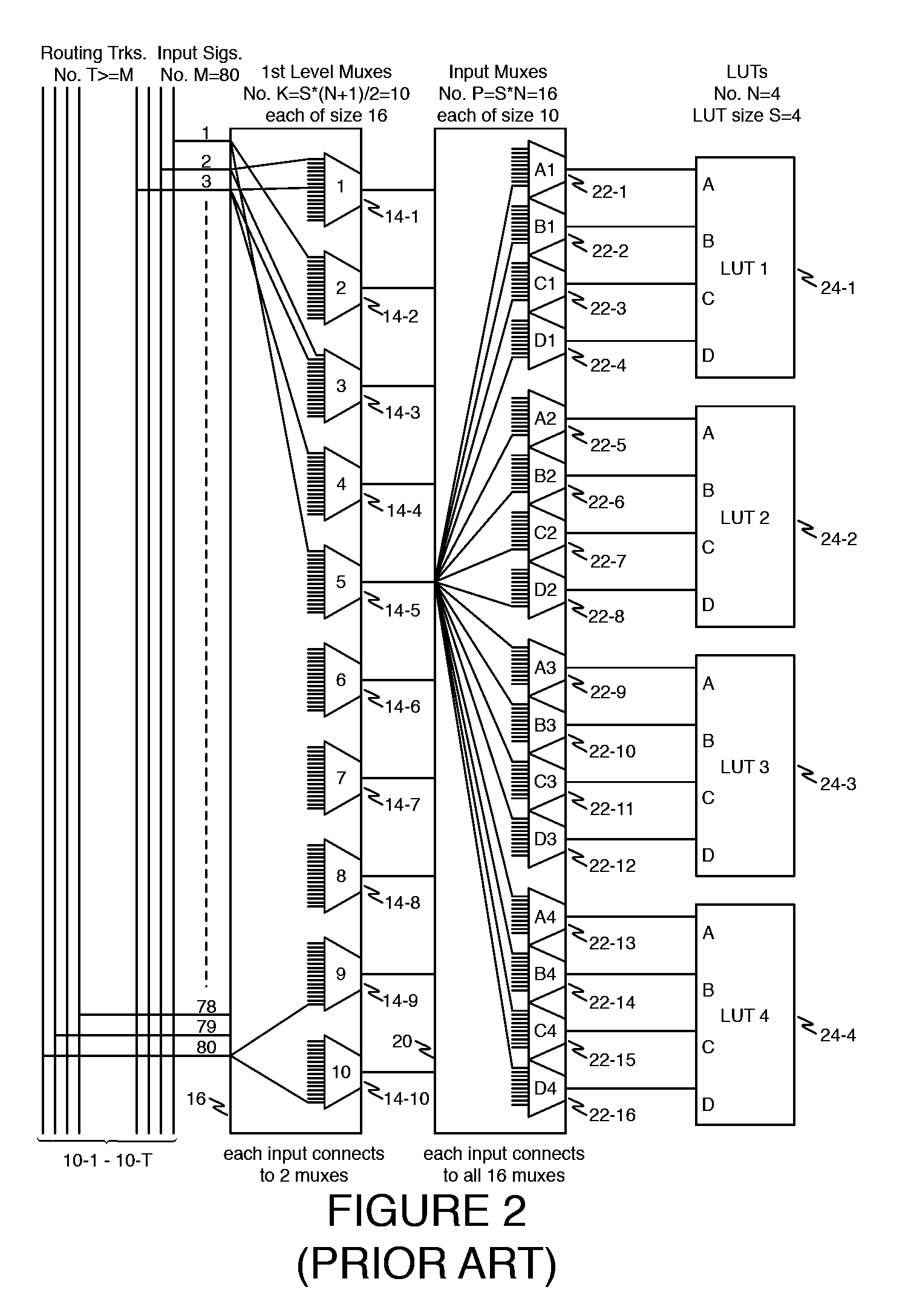
The bandwidth limitation comes from the fact that the number of first-level MUXes K (=(S*(N+1) / 2)) is smaller than the number of LUT input MUXes P (=S*N), which means that N LUTs (i.e., S*N LUT inputs) have to share at most K unique input signals.
The bandwidth limitation is necessary to make the scheme area efficient.
An input bandwidth limitation is the number of unique routing track signals that can be simultaneously routed to the LUT inputs through a cluster input interconnect.
A VPR-type architecture usually assumes full population in the second crossbar, which is very area expensive.
The research has concluded that having K>=S*N number of first-level MUXes in such a scheme (i.e., no bandwidth limitation, or allowing all LUT inputs to have unique input signal) is excessive and therefore a waste of resources.
This method can only be used for a one-level crossbar.

Method used


Image

  • FPGA architecture having two-level cluster input interconnect scheme without bandwidth limitation
  • FPGA architecture having two-level cluster input interconnect scheme without bandwidth limitation
  • FPGA architecture having two-level cluster input interconnect scheme without bandwidth limitation

Examples


Embodiment Construction

[0024]Persons of ordinary skill in the art will realize that the following description of the present invention is illustrative only and not in any way limiting. Other embodiments of the invention will readily suggest themselves to such skilled persons.

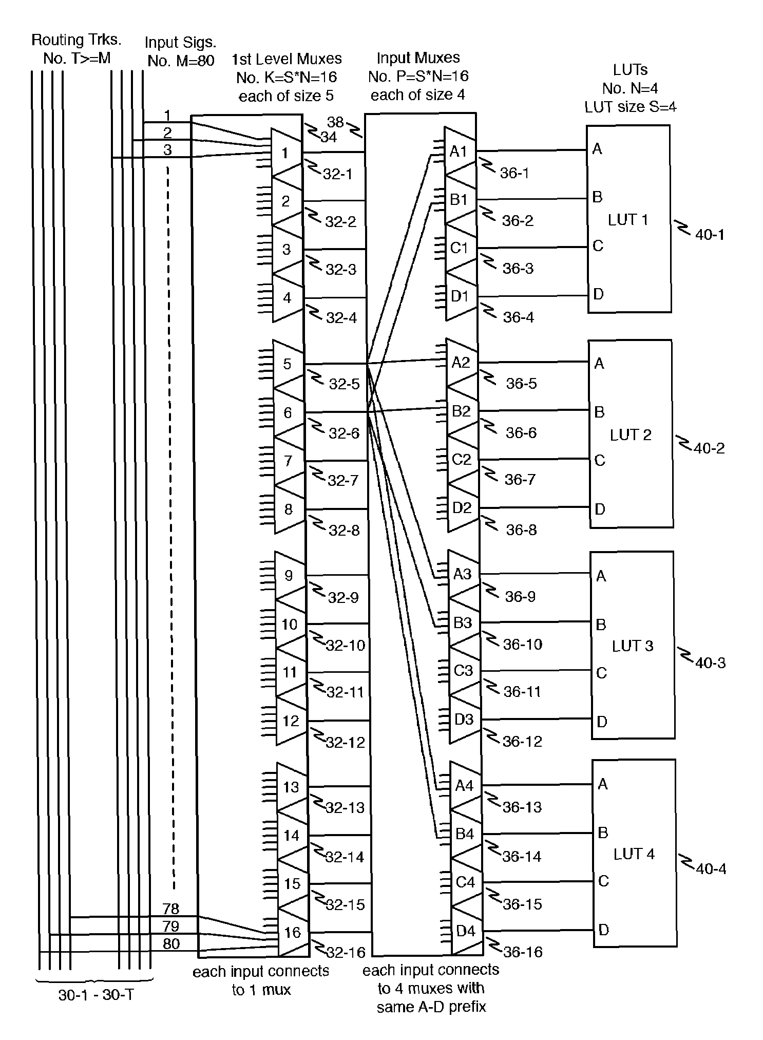
[0025]An illustrative embodiment of the present invention as shown in FIG. 3 includes an interconnect scheme for routing tracks to inputs of logic cells in a cluster-based programmable logic architecture that has two multiplexer levels. The interconnect scheme of the present invention has no bandwidth limitation; that is, a unique signal can be brought in for every logic cell input. In another embodiment the architecture may have a limited bandwidth limitation that is greatly reduced compared to the prior art.

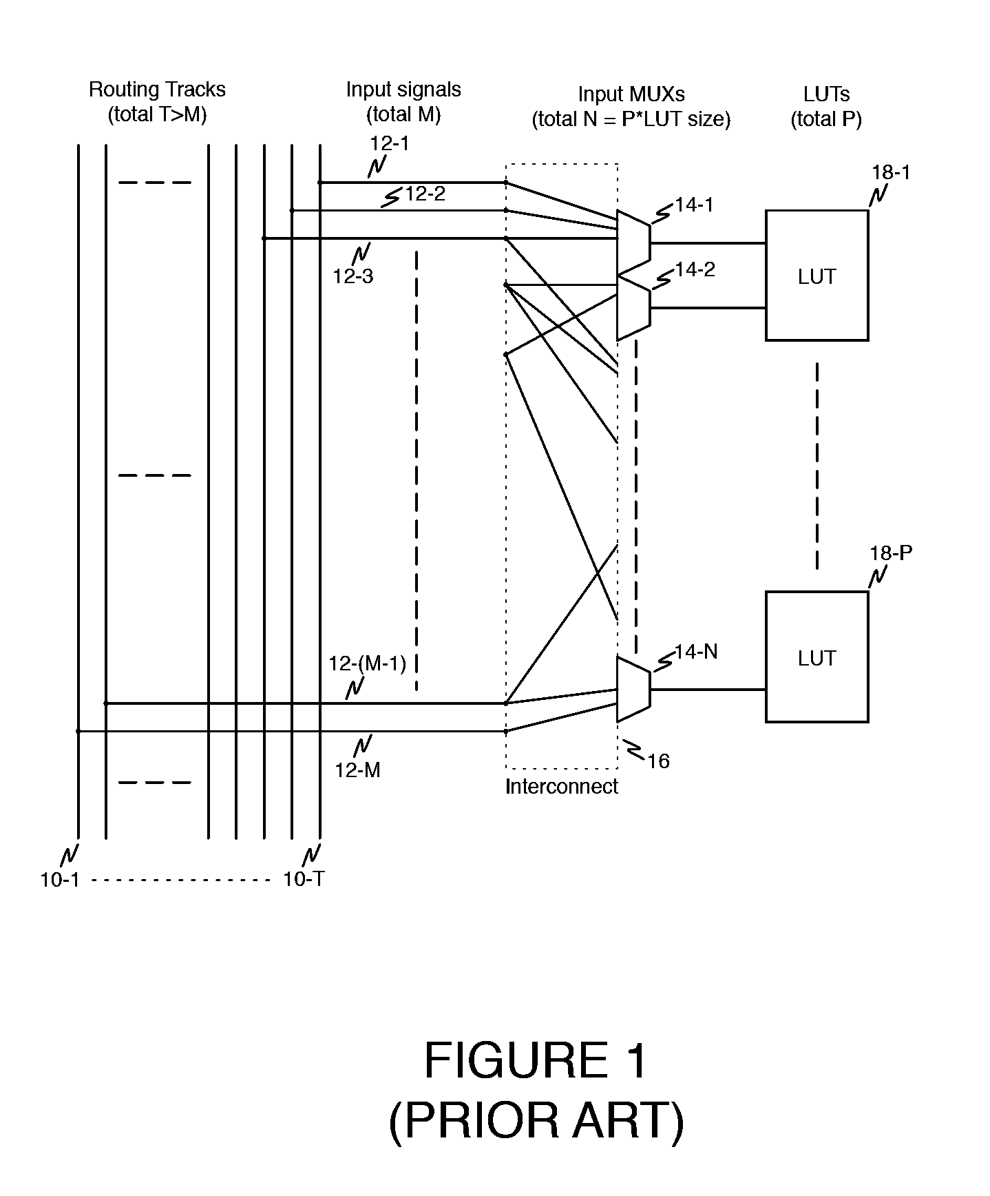
[0026]Referring now to FIG. 3, a block diagram shows an illustrative example of a two-level input interconnect scheme according to the present invention. As in the schemes shown in FIGS. 1 and 2, the two-level interconnect scheme...


PUM


Abstract

An interconnect architecture for a programmable logic device comprises a plurality of interconnect routing lines. The data inputs of a plurality of first-level multiplexers are connected to the plurality of interconnect routing lines such that each interconnect routing line is connected to only one multiplexer. A plurality of second-level multiplexers are organized into multiplexer groups. Each of a plurality of lookup tables is associated with one of the multiplexer groups and has a plurality of lookup table inputs. Each lookup table input is coupled to the output of a different one of the second-level multiplexers in the one of the multiplexer groups with which it is associated. The data inputs of the second-level multiplexers are connected to the outputs of the first-level multiplexers such that each output of each first-level multiplexer is connected to an input of only one second-level multiplexer in each multiplexer group.

Description

CROSS-REFERENCE TO RELATED APPLICATIONS[0001]This application claims priority to U.S. Provisional Patent Application Ser. No. 60 / 825,872, filed Sep. 15, 2006.BACKGROUND OF THE INVENTION[0002]1. Field of the Invention[0003]The present invention relates to field programmable gate array (FPGA) architectures. More specifically, the invention relates to an area efficient interconnect scheme for a cluster based FPGA architecture that connects inter-cluster routing tracks to the inputs of look-up tables (or other logic cells) in the cluster.[0004]2. The Prior Art[0005]A cluster architecture is a type of FPGA architecture in which the basic repeating layout tile is a cluster. The cluster is an aggregation of logic blocks and routing multiplexers. Usually, a limited number of inputs are provided into the cluster in order to save area. A routing multiplexer is a basic FPGA routing element with multiple inputs and one output. It can be programmed to connect one of its inputs to the output. The...

Claims


Application Information

Patent Timeline
IPC IPC(8): H01L25/00H03K19/177
CPCH03K19/17736
Inventor FENG, WENYIKAPTANOGLU, SINAN
Owner MICROSEMI SOC
Learn More