

Nitride semiconductor light emitting element and method for manufacturing nitride semiconductor
a light emitting element and semiconductor technology, applied in semiconductor devices, nanotechnology, electrical equipment, etc., can solve the problems of difficult manufacturing difficult to achieve the manufacture of devices using such semiconductors, and extremely poor surface morphology, etc., to achieve less lattice failure, less distortion due to heat, and high crystal quality
- Summary
- Abstract
- Description
- Claims
- Application Information
AI Technical Summary
Benefits of technology
Problems solved by technology
Method used
Image

Examples
Embodiment Construction
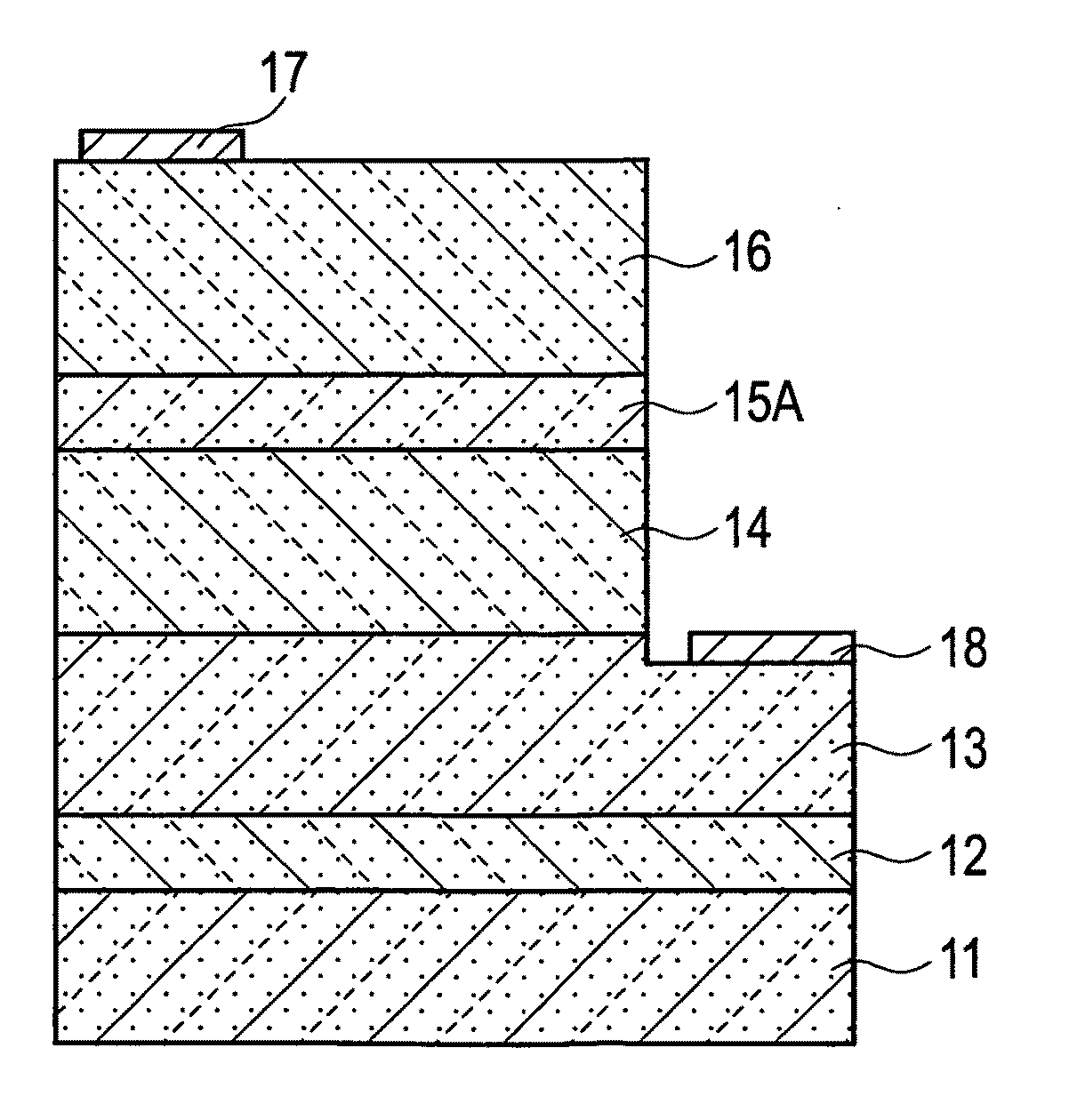
[0103]An embodiment of the present invention will be described hereinbelow with reference to drawings. FIG. 1 shows an example of a structure of a nitride semiconductor light emitting element according to the present invention.
[0104]A sapphire substrate 1 is used as a growing substrate, and an AlN buffer layer 2 is formed on the sapphire substrate 1. On the AlN buffer layer 2, nitride semiconductors of an n-type AlGaN layer 3, an InGaN / GaN active layer 4, and a p-type GaN layer 6 are layered in this order. These nitride semiconductors are formed by the known MOCVD method or the like. The nitride semiconductor here indicates an AlGaInN quaternary mix crystal, which is so called a III-V nitride semiconductor, and can be expressed as AlxGayInzN (x+y+z=1, 0≦x≦1, 0≦y≦1, 0≦z≦1).
[0105]Further, mesa etching is performed from the p-type GaN layer 6 until the n-type AlGaN layer 3 is exposed and an n electrode 8 is formed on the surface of the exposed n-type AlGaN layer 3. Meanwhile, a p elect...
PUM
 Abstract
Description
Claims
Application Information