Memory systems and methods for dynamically phase adjusting a write strobe and data to account for receive-clock drift

Active Publication Date: 2011-05-24
RAMBUS INC
View PDF56 Cites 51 Cited by
  • Summary
  • Abstract
  • Description
  • Claims
  • Application Information

AI Technical Summary

Problems solved by technology

Designing a memory controller that provides the write DQS within a timing window tDQSS can be complicated by the fact that the memory controller is desired to operate in many different system topologies.
For example, relatively short, lightly loaded channels may lead a DQS to arrive too early; whereas relatively long, highly loaded channels may lead a DQS to arrive too late.
In either case, the early or late DQS may violate the specification requirement for the timing window tDQSS, a

Method used


Image

  • Memory systems and methods for dynamically phase adjusting a write strobe and data to account for receive-clock drift
  • Memory systems and methods for dynamically phase adjusting a write strobe and data to account for receive-clock drift
  • Memory systems and methods for dynamically phase adjusting a write strobe and data to account for receive-clock drift

Examples


Embodiment Construction

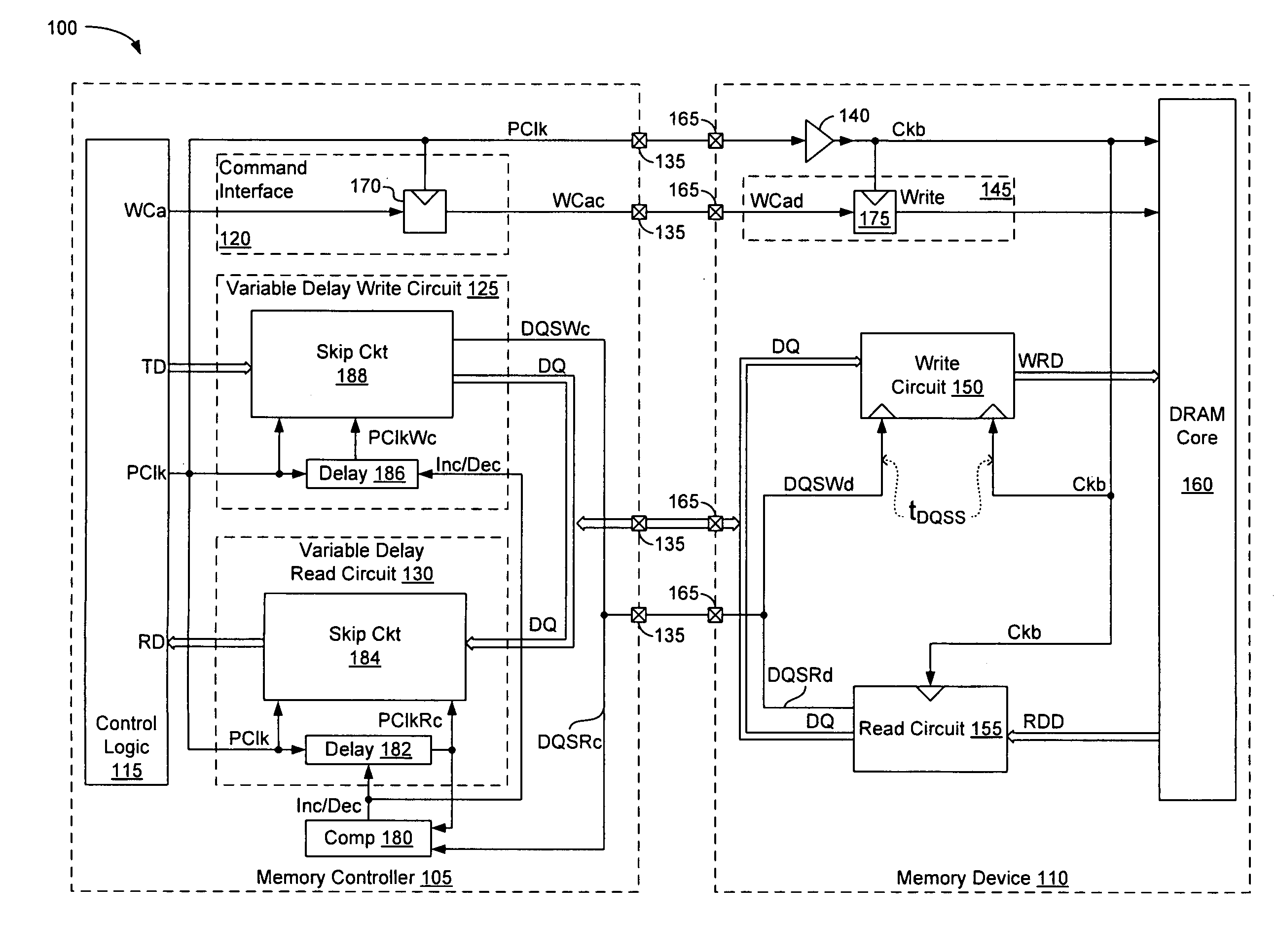
FIG. 1 depicts a memory system 100, including a memory controller 105 and at least one memory device 110. In accordance with the depicted embodiment, memory controller 105 adaptively controls the timing of the write DQS to compensate for timing drift of write signals within memory device 110, and therefore to prevent violations of the tDQSS timing window. Read DQS signals from memory device 110 provide a measure of write-signal timing. Memory controller 105 monitors the phase of read DQS signals to sense and correct for write-signal drift.

Memory controller 105 includes control logic 115 that issues address and control signals to a command interface 120, conveys byte-wide transmit-data signals TD to a variable-delay write circuit 125, and receives byte-wide receive-data signals RD from a variable delay read circuit 130. A distributed clock signal PClk defines the clock domain for control logic 115, interface 120, and portions of variable-delay write and read circuits 125 and 130. Res...


PUM


Abstract

A memory system includes a memory controller that writes data to and reads data from a memory device. A write data strobe accompanying the write data indicates to the memory device when the write data is valid, whereas a read strobe accompanying data from the memory device indicates to the memory controller when the read data is valid. The memory controller adaptively controls the phase of the write strobe to compensate for timing drift at the memory device. The memory controller uses the read strobe as a measure of the drift.

Description

FIELDThe subject matter disclosed herein relates generally to circuits for communicating data between integrated circuits, and in particular to circuits and associated methods for phase shifting data and strobe signals to accommodate drift in a clock signal.BACKGROUNDSDRAM, or synchronous dynamic random access memory, is a type of memory integrated circuit that waits for rising or falling edges of a timing reference signal before responding to control inputs. Typical examples of timing reference signals include clock signals and strobe signals. DDR SDRAM, or double-data-rate SDRAM, achieves greater bandwidth than ordinary SDRAM by transferring data on both the rising and falling edges of timing reference signals.Many DDR SDRAMs that produce data also produce a data strobe, called “DQS” (“data query strobe”), to indicate that data is valid. The DQS is transmitted, along with data, from the memory controller to the DDR SDRAM during write operations and from the DDR SDRAM from the memo...

Claims


Application Information

Patent Timeline
IPC IPC(8): G11C7/00
CPCG06F13/1689G11C29/02G11C29/022G11C29/023G11C29/50012G11C11/40615G11C29/028G11C7/1051G11C7/22G11C7/1072G11C7/04G11C11/4076G11C11/409
Inventor WARE, FREDERICK A.
Owner RAMBUS INC
Why Eureka
Try Eureka