Method for manufacturing a MOSFET with a surrounding gate of bulk Si

Active Publication Date: 2011-06-14
INST OF MICROELECTRONICS CHINESE ACAD OF SCI
View PDF2 Cites 2 Cited by
  • Summary
  • Abstract
  • Description
  • Claims
  • Application Information

AI Technical Summary

Benefits of technology

[0015]The present invention provides a method for manufacturing the bulk Si surrounding-g

Problems solved by technology

The main difficulty in manufacturing surrounding-gate devices on the bulk Si is to form the sacrificing layer.
The currently few reports on the manufacturing method based on the bulk Si substrate either need the Damascus replaced gate, which uses complex and expensive SiGe epitaxy as the sacrificing layer, or directly perform isotropic etching on the Si, which causes contamination of the substrate.
Further

Method used


Image

  • Method for manufacturing a MOSFET with a surrounding gate of bulk Si
  • Method for manufacturing a MOSFET with a surrounding gate of bulk Si
  • Method for manufacturing a MOSFET with a surrounding gate of bulk Si

Examples


Example

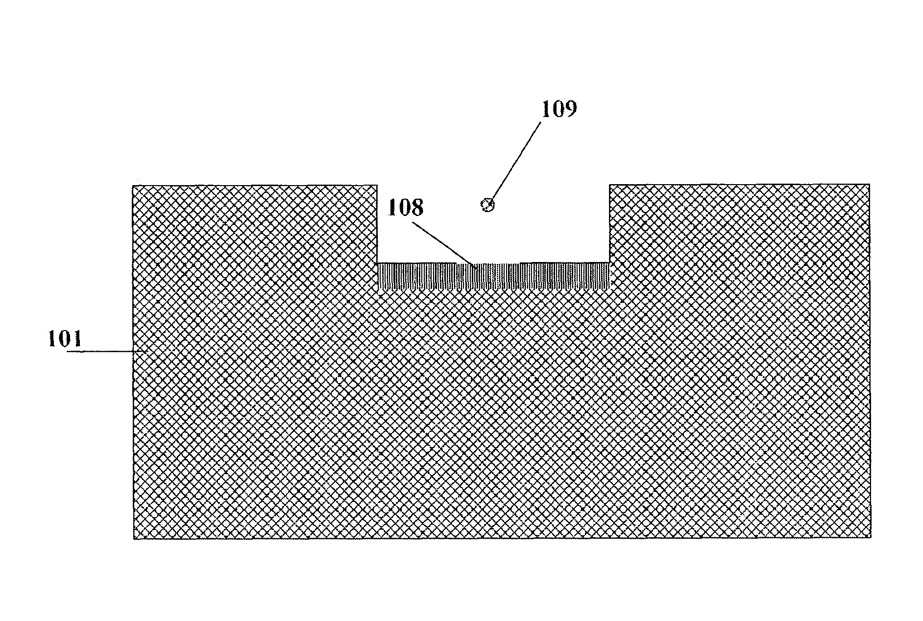
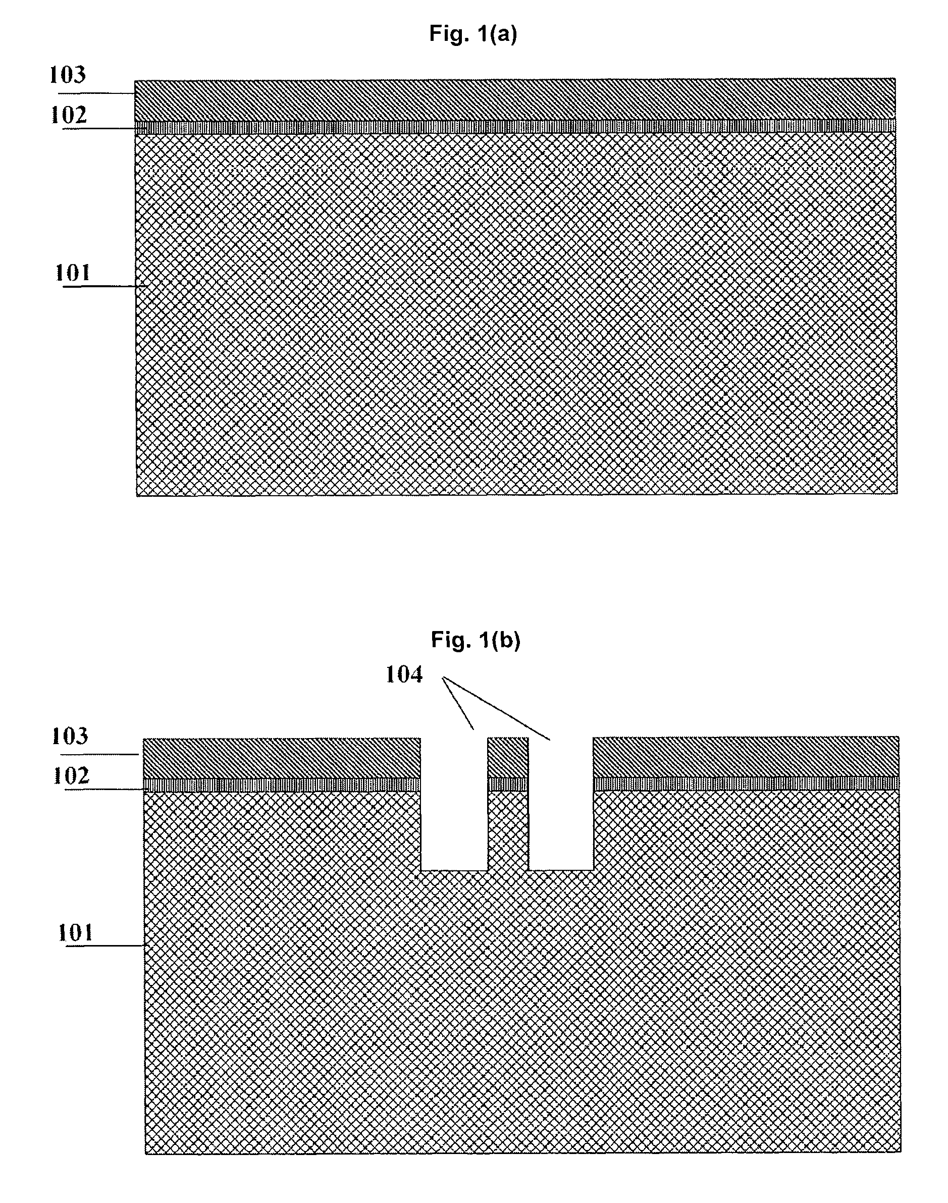
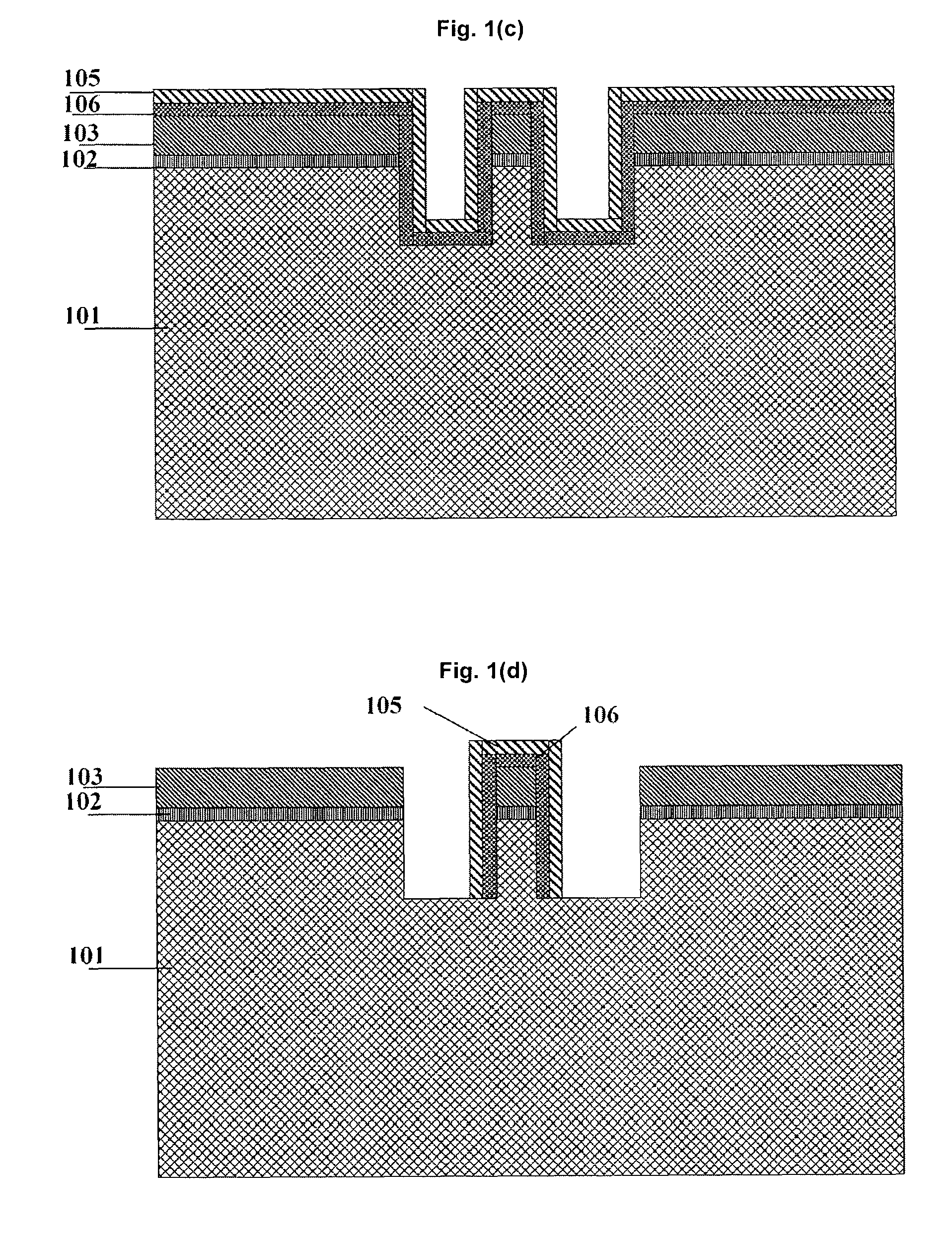
[0059]Reference signs in the drawings:

[0060]101Si substrate;102buffer SIO2 oxide layer;103SiN dielectric layer;104two adjacent slots;105SiN sidewall;106sidewall buffer SIO2 oxide layer;107SiO2 oxide layer of the first oxidation;108SiO2 oxide layer of the second oxidation;109Si nanowire;110oxide (TEOS or LTO) dielectric layer;201layout of active region;202layout of adjacent slots;203layout of gate; and204layout of contact.

DETAILED DESCRIPTION OF THE PREFERRED EMBODIMENTS

[0061]The steps of the method according to the present invention are as follows:[0062]1) performing double-well process and driving the dopants into the substrate;[0063]2) forming LOCal Oxidation of Silicon (LOCOS) isolation or Shallow Trench Isolation (STI);[0064]3) depositing a buffer SiO2 oxide layer / SiN dielectric layer;[0065]4) performing positive electron beam exposure, and etching to form slots;[0066]5) isotropically depositing a buffer SiO2 oxide layer and a SiN film, and anisotropically etching them to form s...


PUM


Abstract

A method for manufacturing a bulk Si nanometer surrounding-gate MOSFET based on a quasi-planar process, including: local oxidation isolation or shallow trench isolation; depositing buffer SiO2 oxide layer/SiN dielectric layer on the bulk Si; electron beam exposure; etching two adjacent slots; depositing SiN sidewalls; isotropically etching Si; dry oxidation; removing SiN by wet etching; forming the nanowire by stress self-constraint oxidation; depositing and anisotropically etching oxide dielectric layer and planarizing surface; releasing the nanowire by wet etching while keeping sufficiently thick SiO2 at bottom as isolation; growing gate dielectric and depositing gate material; etching back the gate and isotropically etching the gate material by using the gate dielectric as a block layer; shallow implantation in the source/drain region; depositing and etching sidewalls; deep implantation in the source/drain region to form contact. The present invention eliminates self-heating effect and floating-body effect, and is easy to integrate. The present invention is also advantageous in suppression of short channel effect and enables the size of the MOSFET to be smaller.

Description

PRIORITY APPLICATION(S)[0001]This patent application is a continuation of prior International Number PCT / CN2010 / 074699, filed Jun. 29, 2010; which international patent application claims the benefit of priority, under 35 U.S.C. §119, to Chinese Patent Application Serial Number 200910243780.1, filed Dec. 24, 2009, the entire contents of which are incorporated herein by reference in their entirety.FIELD OF THE INVENTION[0002]The invention relates to a technical field of a microelectronic nanometer-scale Complementary Metal Oxide Semiconductor (CMOS) device and Very Large Scale Integrated Circuits, and in particular, to a method for manufacturing a bulk Si surrounding gate Metal Oxide Semiconductor Field Effect Transistor (MOSFET) based on quasi-planar process.DESCRIPTION OF THE PRIOR ART[0003]Nanometer CMOS devices are developed according the Moore Rule. As the continuous scaling of the size of a planar bulk Si device has encountered a serious challenge, various devices with new struc...

Claims


Application Information

Patent Timeline
IPC IPC(8): H01L21/336
CPCB82Y10/00B82Y40/00H01L29/0665H01L29/66439H01L29/775H01L29/0673Y10S977/938Y10S977/762H01L29/42392H01L29/78696
Inventor SONG, YIZHOU, HUAJIEXU, QIUXIA
Owner INST OF MICROELECTRONICS CHINESE ACAD OF SCI
Why Eureka
Try Eureka