Light emitting diode package having flexible PCT directly connected to light source

a technology of light emitting diodes and flexible pcts, which is applied in the direction of electrical equipment, lighting and heating equipment, lighting protection devices, etc., can solve the problems of deterioration of quality or reliability, reduced thickness, and reduced so as to reduce the total height of led packages and ensure the thickness of flanges. , the effect of high reliability

Inactive Publication Date: 2011-06-21
AVAGO TECH INT SALES PTE LTD
View PDF3 Cites 9 Cited by
  • Summary
  • Abstract
  • Description
  • Claims
  • Application Information

AI Technical Summary

Benefits of technology

[0009]A conventional light emitting diode package structure as shown in FIG. 8 requires the lead frame 85 for soldering the LED 82 to the FPCB 87, in addition to the rigid PCB 88. Further, when the lead frame 85 is mounted on the FPCB 87, it is necessary to bend the lead frame 85 at such a large angle as to prevent cracks or the like, which requires the flange 84 to have a relatively large thickness. Therefore, a light emitting diode package that includes a rigid PCB in addition to a light emitting diode comprising a lens (encapsulant), a flange, and a lead frame, has a relatively large total height. This is a problem for thickness reduction of a mobile device that has to mount a light emitting diode package with a construction shown in the figure.
[0012]For a conventional light emitting diode package utilizing a lead frame for connecting an LED to an FPCB, it is difficult to reduce the total height of the light emitting diode package. For example, one component constituting a light emitting diode package is a lens formed of an encapsulant, and height reduction of the lens reduces the brightness of the LED. Further, a flange is used as other component, and the flange has to have a certain level of thickness in relation with a bending angle of the lead frame as described above. It is therefore difficult to reduce the height of the flange.
[0013]One object of the present invention is to reduce the height of a light emitting diode package by eliminating a rigid PCB and a lead frame, thereby to reduce a size of a device carrying the LED.
[0014]Another object of the present invention is to avoid an operational defect of an LED attributable to heat generated by soldering a lead frame to a rigid PCB, thereby to improve the quality and reliability of the LED.
[0017]The present invention does not require a lead frame for electrically connecting an LED to an FPCB, and thereby a certain level thickness of a flange, which is necessary for bending a lead frame, can be reduced. Further, a rigid PCB as a supporting plate for mounting and soldering an LED onto an FPCB is not necessary, thereby enabling the reduction of the total height of an LED package.
[0018]Further, the present invention does not require soldering of a lead frame to an FPCB, resulting in no heat generation associated with the soldering. This enables highly reliable electrical connection, thereby improving the quality and reliability of LED. Further, it is possible to eliminate the above-mentioned design constraints on components attributable to soldering heat.

Problems solved by technology

This is a problem for thickness reduction of a mobile device that has to mount a light emitting diode package with a construction shown in the figure.
In addition, heat generated by soldering the lead frame 85 to the FPCB 87 may cause operational defects such as deterioration of optical output and no lighting of the LED 82, thereby leading to deterioration in quality or reliability.
An operational defect of this type is caused by exfoliation of an encapsulation resin from an LED chip or wire cutting, which is attributed to a fact that the thermal expansion degree of the encapsulation resin by soldering heat is varied depending on the location.
These constraints creates barriers to develop LEDs having new shapes or structures, for example, an ultra-compact LED susceptible to thermal influence.
For a conventional light emitting diode package utilizing a lead frame for connecting an LED to an FPCB, it is difficult to reduce the total height of the light emitting diode package.
For example, one component constituting a light emitting diode package is a lens formed of an encapsulant, and height reduction of the lens reduces the brightness of the LED.
It is therefore difficult to reduce the height of the flange.

Method used


Image

  • Light emitting diode package having flexible PCT directly connected to light source
  • Light emitting diode package having flexible PCT directly connected to light source
  • Light emitting diode package having flexible PCT directly connected to light source

Examples


Embodiment Construction

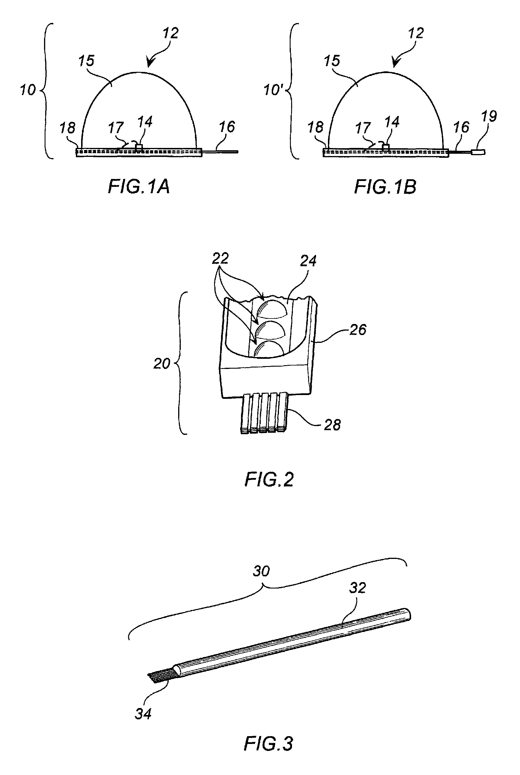
[0029]Hereafter, some embodiments of LED packages wherein LED chips are connected to FPCBs without lead frames will be described by referring to the drawings.

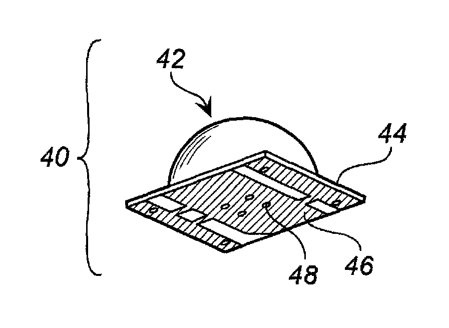
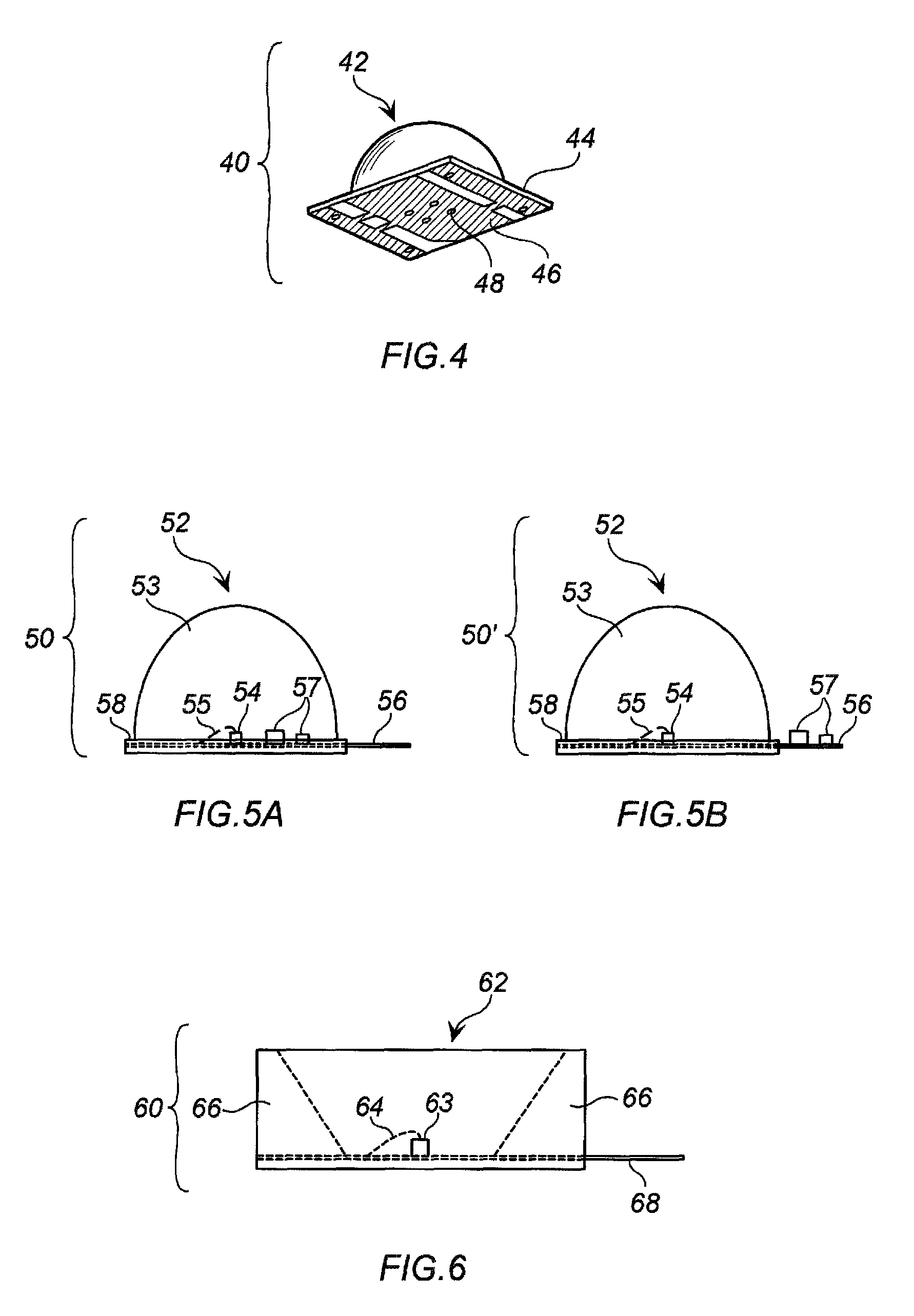
[0030]FIGS. 1A and 1B are side views showing LED packages 10 and 10′, respectively, according to one embodiment of the present invention. An LED 12 has a structure similar to a conventional one (but a lead frame is excluded), which comprises an LED chip 14, an encapsulant 15 (encapsulation resin), a wire 17, and a flange 18. The package includes an FPCB 16 and a connector 19. In FIGS. 1A and 1B, like reference numerals refer to portions for which the same components are usable. In either structure, the FPCB is directly connected to the LED chip by a conductive resin or soldering, and a bonding wire as shown in FIG. 7. This direct connection can be achieved, for example, by: applying an epoxy resin containing silver paste to a location on the FPCB for mounting the LED chip; curing the resin in a high-temperature furnace after mo...


PUM


Abstract

A light emitting diode package comprising a substrate electrically connectable to an external unit with a reduced height. A flexible PCB for electrical connection between a light emitting diode and the external unit is directly connected to a light emitting element. The direct connection is conducted by applying a conductive resin to an electrode on the flexible PCB, on which the light emitting element is mounted; mounting the light emitting element; curing the conductive resin in a high-temperature furnace. The present invention requires neither a lead frame for electrical connection of the light emitting element to the flexible PCB nor a rigid PCB for supporting the flexible PCB, thus reducing the total height of the light emitting diode package.

Description

[0001]This application claims priority from Japanese Patent Application Number 2006-289,444, filed Oct. 25, 2006, of Akira Takekuma and Chew Tong Fatt, which is hereby incorporated by reference for all that is disclosed herein.BACKGROUND OF THE INVENTION[0002]1. Field of the Invention[0003]The present invention relates to a light emitting diode package structure, and particularly relates to a structure for electrically connecting a light emitting diode to an external unit via a flexible PCB.[0004]2. Description of Related Art[0005]Compact electrical devices typified by mobile devices such as recent digital still cameras and mobile phones, often employ a flexible print circuit board (hereafter referred to as “FPCB”) as substrates for electrical connection between units or circuits for reduction in size and weight. Relatively small and light components such as chip components are sometimes directly soldered on FPCBs. For soldering an LED on an FPCB, a surface mount LED is generally us...

Claims


Application Information

Patent Timeline
Patent Type & Authority Patents(United States)
IPC IPC(8): F21S4/00F21V21/00H01L33/58H01L33/62
CPCH01L33/62H01L2224/48091H01L2224/48227H01L2224/48465H01L2224/73265H01L2924/01079H01L2224/45144H05K1/189H01L2224/32225H01L2924/00014H01L2924/00
Inventor TAKEKUMA, AKIRAFATT, CHEW TONG
Owner AVAGO TECH INT SALES PTE LTD
Why Eureka
Try Eureka