Substrate and semiconductor device

a technology of semiconductor devices and substrates, applied in the direction of printed circuits, sustainable manufacturing/processing, final product manufacturing, etc., can solve the problems of limiting the design and materials of packages, affecting the design of insulating films, and affecting the performance of substrates, etc., to achieve the effect of adjusting the height of bump electrodes

Inactive Publication Date: 2007-07-19
RENESAS ELECTRONICS CORP
View PDF1 Cites 33 Cited by
  • Summary
  • Abstract
  • Description
  • Claims
  • Application Information

AI Technical Summary

Benefits of technology

[0045]As has been described in the above, the present invention can readily adjust the height of the bump electrodes to be bonded to the lands on the substrates.

Problems solved by technology

In this sort of PoP technology, there has conventionally been concerned that warping generated in the packages may result in bonding failure between the packages.
This sort of problem is ascribable to difference in the thermal expansion coefficients depending on configurations of the individual packages.
Any efforts of ensuring a desirable bonding have occasionally limited the package design and materials.
It has, therefore, been anticipated that design of the insulating film is more complicated.

Method used


Image

  • Substrate and semiconductor device
  • Substrate and semiconductor device
  • Substrate and semiconductor device

Examples


first embodiment

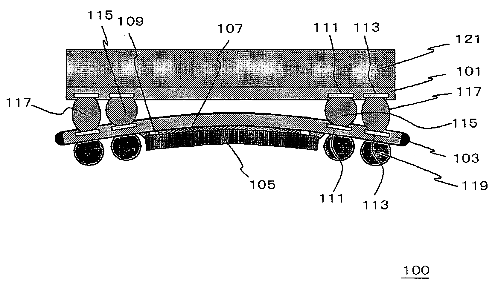
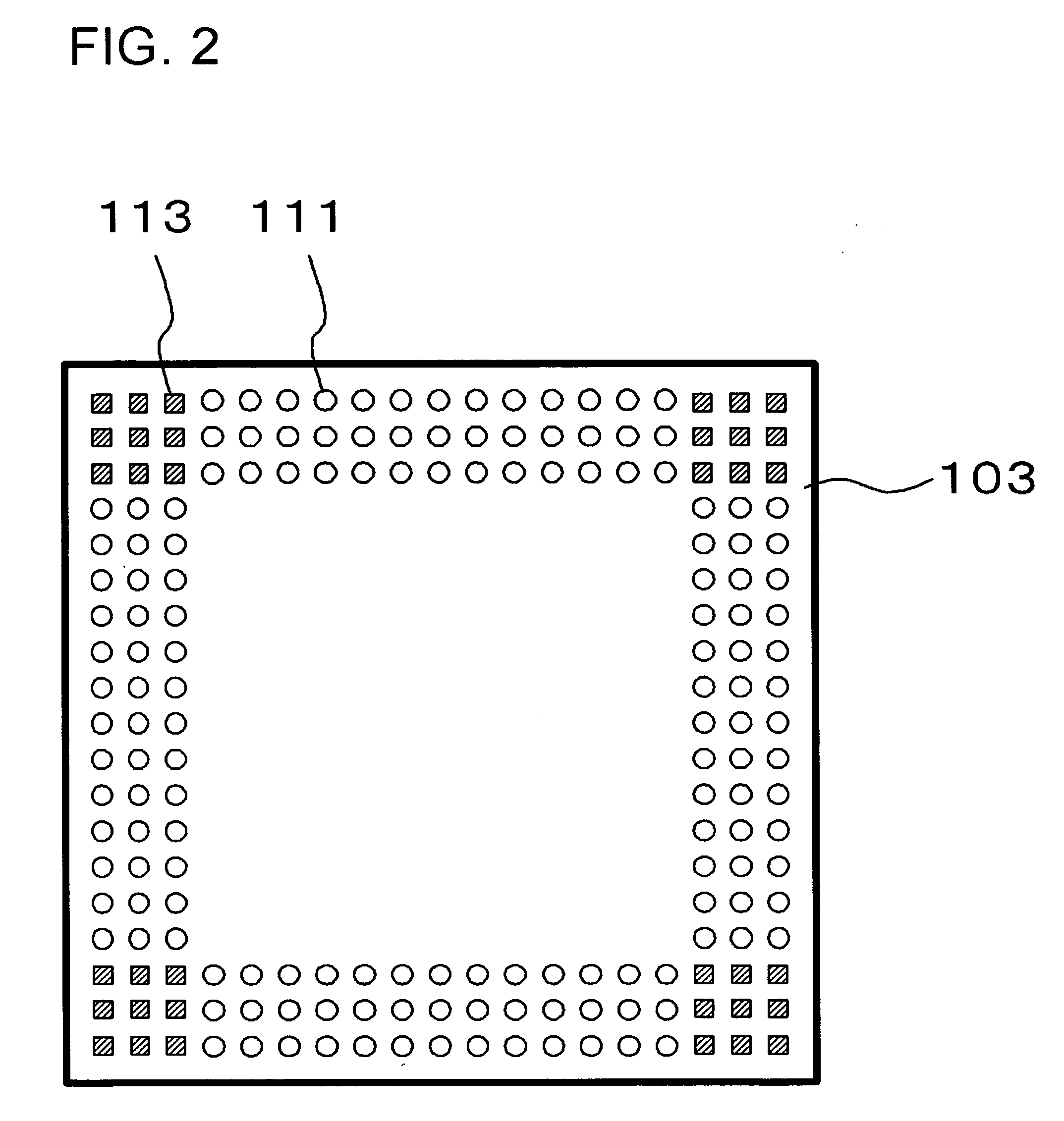
[0064]FIG. 1 is a sectional view showing a configuration of a semiconductor device of this embodiment. FIG. 2 is a plan view showing a plane geometry and arrangement of the lands on the first interconnect substrate 103 of the semiconductor device shown in FIG. 1. Also the plane geometry and plane arrangement of the lands on the second interconnect substrate 101 may be same as those shown in FIG. 2.

[0065]A semiconductor device 100 shown in FIG. 1 includes a first substrate (first interconnect substrate 103), a second substrate (second interconnect substrate 101) provided so as to oppose with one surface of the first interconnect substrate 103, and a semiconductor chip 105 mounted on the second interconnect substrate 101 or on the first interconnect substrate 103. FIG. 1 shows that the semiconductor chip 105 is mounted on the first interconnect substrate 103, so that the first interconnect substrate 103 and the semiconductor chip 105 are stacked.

[0066]The first interconnect substrate ...

second embodiment

[0100]The semiconductor device 100 shown in FIG. 1 dealt with the case where the gap between the substrates is large at four corners, whereas another possible configuration is such as having a large gap at the center of the substrates.

[0101]FIG. 10 is a sectional view showing a configuration of a semiconductor device of this embodiment. FIG. 11 is a drawing showing a plane geometry of the surface, opposed with the first interconnect substrate 103, of the second interconnect substrate 101 of the semiconductor device shown in FIG. 10. Also the plane geometry and plane arrangement of the lands in the second interconnect substrate 101 may be same as those in the configuration shown in FIG. 10. A basic configuration of the semiconductor device shown in FIG. 10 and FIG. 11 is similar to that of the semiconductor device 100 in the first embodiment, except that the arrangement of the first lands 111 and the second lands 113 is inverted.

[0102]More specifically, the plane geometry of the firs...


PUM


Abstract

Aiming at adjusting the height of bump electrodes connected to lands on a substrate, a semiconductor device 100 has a first interconnect substrate 103 and a second interconnect substrate 101. On one surface of these substrates, first lands 111 and second lands 113 are provided. The plane geometry of the second lands 113 is a polygon characterized by the inscribed circle thereof having an area smaller than the area of the inscribed circle of the first land.

Description

[0001]This application is based on Japanese patent application No. 2006-005697 the content of which is incorporated hereinto by reference.BACKGROUND[0002]1. Technical Field[0003]The present invention relates to a substrate on which a semiconductor chip is mounted, and a semiconductor device using the same.[0004]2. Related Art[0005]In semiconductor devices, semiconductor chips having a large number of circuit elements such as transistors, resistors, capacitors and so forth formed therein are mounted typically on interconnect substrates. The circuit elements are interconnected so as to allow the semiconductor devices to exhibit circuit operations and functions required thereto. Methods of interconnecting the semiconductor chips and the interconnect substrates include the wire bonding method using gold wires, and the flip-chip bonding method connecting so as to oppose the circuit-formed surfaces with the surfaces of the interconnect substrates.[0006]High-density mounting technologies o...

Claims


Application Information

Patent Timeline
Patent Type & Authority Applications(United States)
IPC IPC(8): H01L23/52
CPCH01L21/563H01L23/3128H01L24/13H01L2225/1058H01L2225/1023H01L2924/15331H01L2924/15321H01L2224/73204H01L2224/32225H01L2224/16225H01L2924/014H01L2924/01033H01L23/49816H01L23/49838H01L24/10H01L25/105H01L2224/13099H01L2924/01075H01L2924/01079H01L2924/15311H01L2924/19041H01L2924/19043H01L2924/3511H05K1/111H05K3/3436H05K2201/09381H05K2201/094H05K2201/09772H05K2201/10734H01L2924/01005H01L2924/01006H01L2924/00012H01L2924/00H01L2224/13H01L2924/181Y02P70/50
Inventor EJIMA, DAISUKE
Owner RENESAS ELECTRONICS CORP
Why Eureka
Try Eureka