Method for fabricating semiconductor device including vertical channel transistor

a technology of vertical channel transistor and semiconductor device, which is applied in the direction of semiconductor devices, electrical appliances, basic electric elements, etc., can solve the problems of phosphoric acid damage to the interlayer insulation layer b>19/b>, and achieve the effect of reducing bridges

Active Publication Date: 2011-06-21
SK HYNIX INC
View PDF11 Cites 5 Cited by
  • Summary
  • Abstract
  • Description
  • Claims
  • Application Information

AI Technical Summary

Benefits of technology

[0013]Embodiments of the present invention are directed to providing a method for fabricating a semiconductor device, which can reduce bridges from occurring at the end of word lines in a padding region when forming word lines in a semiconductor device including vertical channel transistors.
[0014]The embodiments of the present invention are also directed to providing a method for fabricating a semiconductor device, which can reduce bending of pillar structures when forming trenches for buried bit lines in a semiconductor device including vertical channel transistors.

Problems solved by technology

However, the inter-layer insulation layers 19 may be damaged by phosphoric acid.

Method used


Image

  • Method for fabricating semiconductor device including vertical channel transistor
  • Method for fabricating semiconductor device including vertical channel transistor
  • Method for fabricating semiconductor device including vertical channel transistor

Examples


Embodiment Construction

[0026]Other objects and advantages of the present invention can be understood by the following description, and become apparent with reference to the embodiments of the present invention.

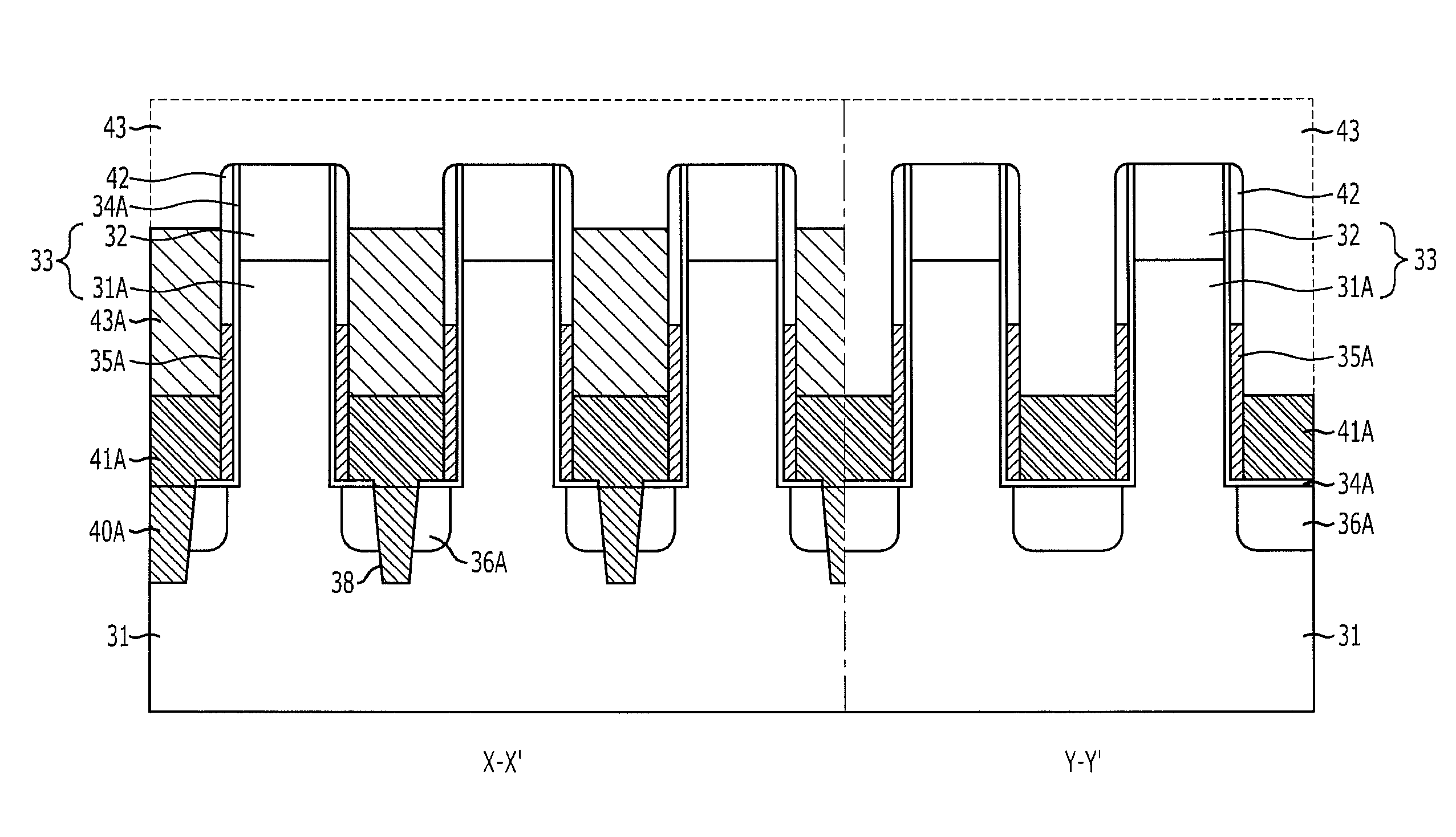
[0027]Embodiments of the present invention relate to a method for fabricating a semiconductor device including a vertical channel transistor. According to the embodiments of the present invention, a damascene pattern formation process for forming word lines may be omitted by forming the word lines by directly patterning a conductive layer, thus improving process efficiency. Furthermore, limitations which may arise while forming damascene patterns may be substantially reduced. Therefore, bridges may be prevented from occurring at the end of word lines in a padding region.

[0028]Moreover, according to the embodiments of the present invention, trenches for forming buried bit lines are formed using a sacrificial layer including borophosphosilicate glass (BPSG) having a smaller intra-layer stress than an ...


PUM


Abstract

A method for fabricating a semiconductor device includes forming a plurality of pillar structures over a substrate, forming gate electrodes over sidewalls of the pillar structures, forming a sacrificial layer buried between the pillar structures, etching the sacrificial layer and the substrate to form trenches in the substrate, forming first inter-layer insulation patterns buried over the trenches and removing the remaining sacrificial layer at substantially the same time, and forming second inter-layer insulation patterns over the first inter-layer insulation patterns and buried between the pillar structures.

Description

CROSS-REFERENCE TO RELATED APPLICATIONS[0001]The present invention claims priority of Korean patent application number 10-2008-0112677, filed on Nov. 13, 2008, the disclosure of which is incorporated by reference in its entirety.BACKGROUND OF THE INVENTION[0002]The present invention relates to a method for fabricating a semiconductor device, and more particularly, to a method for fabricating a semiconductor device including a vertical channel transistor.[0003]The size of cells integrated on a substrate is becoming smaller as semiconductor devices are becoming highly integrated. A transistor in a gigabyte dynamic random access memory (DRAM) device generally requires a size of approximately 4F2, wherein F represents the minimum feature size. Thus, vertical channel transistor has been introduced as a way to increase the efficiency of cells by increasing the integration scale of a DRAM device as well as securing the channel length of the transistor. The vertical channel transistor inclu...

Claims


Application Information

Patent Timeline
Patent Type & Authority Patents(United States)
IPC IPC(8): H01L21/336
CPCH01L27/10876H01L29/7827H01L29/66666H10B12/053
Inventor KANG, SANG-KIL
Owner SK HYNIX INC
Why Eureka
Try Eureka