X-ray detection panel and X-ray detector

a detection panel and detector technology, applied in the direction of x/gamma/cosmic radiation measurement, instruments, radioation controlled devices, etc., can solve the problem of incurred costs whenever x-rays are radiated, and achieve the effect of reducing the frequency of disconnection

Active Publication Date: 2011-07-26
SAMSUNG DISPLAY CO LTD
View PDF16 Cites 5 Cited by
  • Summary
  • Abstract
  • Description
  • Claims
  • Application Information

AI Technical Summary

Benefits of technology

[0026]By using an X-ray detection panel, X-rays can be detected without a separate film by using a PIN diode and by forming two bias connection lines that connect a bias line to the upside and the downside of the panel, even if the bias line is disconnected, and further, X-rays can be detected without an error. Additionally, by forming a bias line with first and second bias lines, occurrences of disconnection can be reduced.

Problems solved by technology

Accordingly, a cost is incurred whenever X-rays are radiated.

Method used


Image

  • X-ray detection panel and X-ray detector
  • X-ray detection panel and X-ray detector
  • X-ray detection panel and X-ray detector

Examples


Embodiment Construction

[0035]Embodiments of the present invention will be described more fully hereinafter with reference to the accompanying drawings.

[0036]In the drawings, the thickness of layers, films, panels, regions, etc., are exaggerated for clarity. Like reference numerals designate like elements throughout the specification. It will be understood that when an element such as a layer, film, region, or substrate is referred to as being “on” another element, it can be directly on the other element or intervening elements may also be present. In contrast, when an element is referred to as being “directly on” another element, there are no intervening elements present.

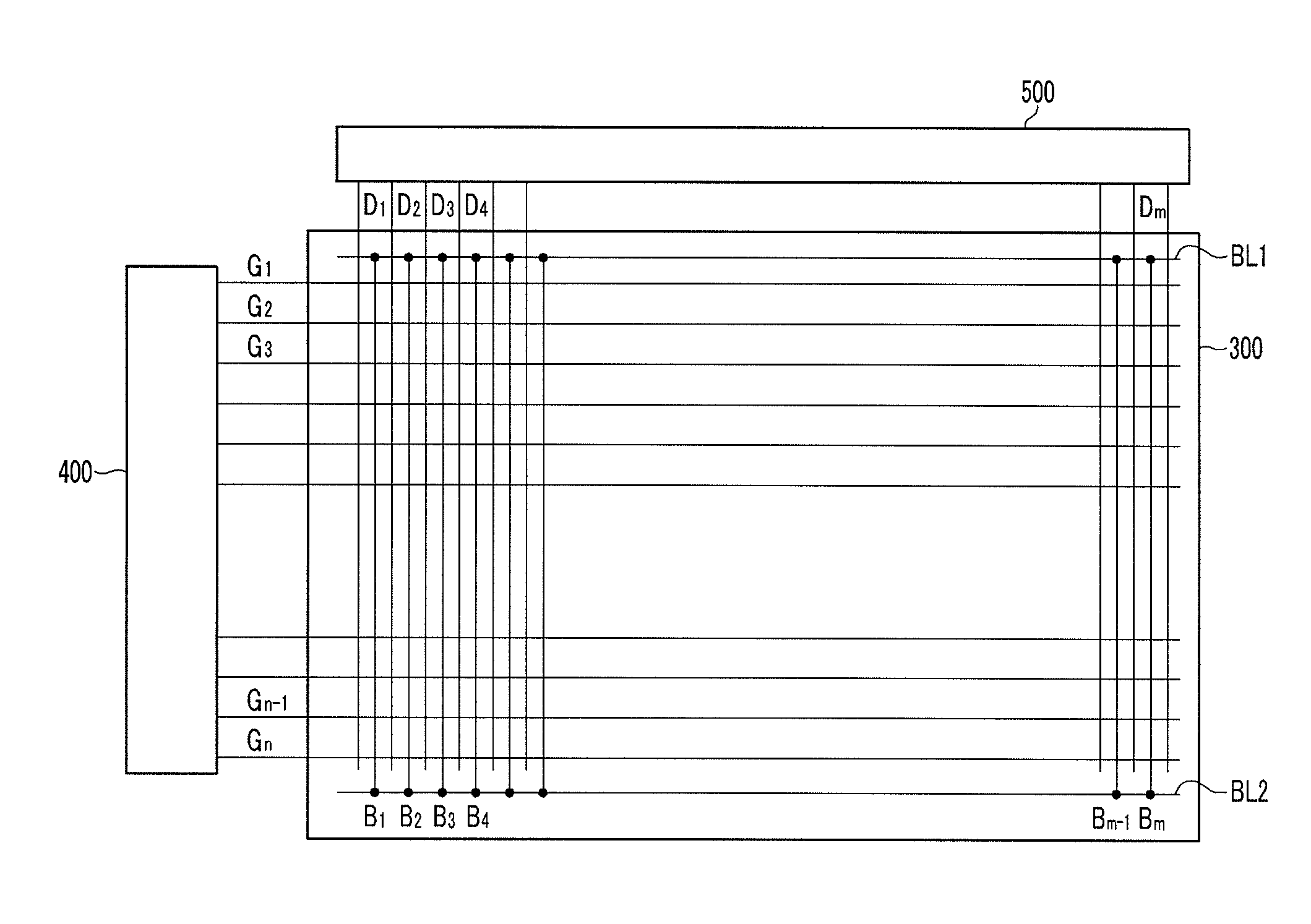
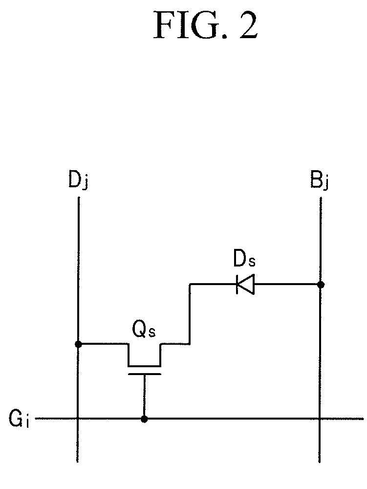
[0037]An X-ray detector according to an exemplary embodiment of the present invention is described in detail with reference to FIGS. 1 and 2.

[0038]FIG. 1 is a diagram illustrating a structure of an X-ray detector according to an exemplary embodiment of the present invention, and FIG. 2 is an equivalent circuit diagram illustrating a detec...


PUM


Abstract

An X-ray detector includes a plurality of bias connection lines that connect both ends, respectively, of a bias line for applying a bias voltage to a PIN diode. The bias line includes first and second bias lines.

Description

CROSS-REFERENCE TO RELATED APPLICATION[0001]This application claims priority to and the benefit of Korean Patent Application No. 10-2008-0085246 filed in the Korean Intellectual Property Office on Aug. 29, 2008, the entire contents of which are herein incorporated by reference.BACKGROUND OF THE INVENTION[0002](a) Field of the Invention[0003]The present invention relates to an X-ray detection panel and an X-ray detector.[0004](b) Description of Related Art[0005]In the field of radiography X-rays are typically detected using a separate film. In a method using separate films, X-rays should be radiated to a subject that does not move, and a new film should be used for each image. Accordingly, a cost is incurred whenever X-rays are radiated.[0006]X-rays may also be detected using a charge-coupled device (CCD) or a complementary metal-oxide semiconductor (CMOS). Due to the small size of a detector that is formed with the CCD or the CMOS, after X-rays are detected, the image needs to be ma...

Claims


Application Information

Patent Timeline
Patent Type & Authority Patents(United States)
IPC IPC(8): G01T1/24
CPCG01T1/2018G01T1/20184H01L31/115A61B6/00G01T1/20G01T1/00
Inventor JUNG, KWAN-WOOKCHOO, DAE-HO
Owner SAMSUNG DISPLAY CO LTD
Why Eureka
Try Eureka