Light emitting device and manufacturing method thereof

a technology of light emitting devices and manufacturing methods, applied in the direction of discharge tubes/lamp details, discharge tubes luminescnet screens, electric discharge lamps, etc., to achieve the effect of reducing the luminance of light emitting elements due to voltage drop of the second electrode in the pixel portion

Inactive Publication Date: 2011-08-09
SEMICON ENERGY LAB CO LTD
View PDF49 Cites 35 Cited by
  • Summary
  • Abstract
  • Description
  • Claims
  • Application Information

AI Technical Summary

Benefits of technology

[0020]By carrying out the present invention, an auxiliary wiring can be formed in the vicinity of a light emitting element. Therefore, it becomes possible to form an auxiliary wiring which is electrically connected to a second electrode not only in a peripheral portion of a light emitting display panel but also in a pixel portion having a light emitting element; therefore, variation in luminance among light emitting elements due to voltage drop of the second electrode in the pixel portion can be reduced.

Problems solved by technology

However, in the case of the above-mentioned Patent Document 1, in order to reduce voltage drop due to the resistance of a connection wiring of a second electrode, the connection wiring for the second electrode is formed at the periphery of a pixel portion, with a wider line width than that of a power supply wiring for light emission, which is not favorable when it is desired to decrease a non-active area of the panel (when it is desired to reduce the frame size).

Method used


Image

  • Light emitting device and manufacturing method thereof
  • Light emitting device and manufacturing method thereof
  • Light emitting device and manufacturing method thereof

Examples


embodiment mode 1

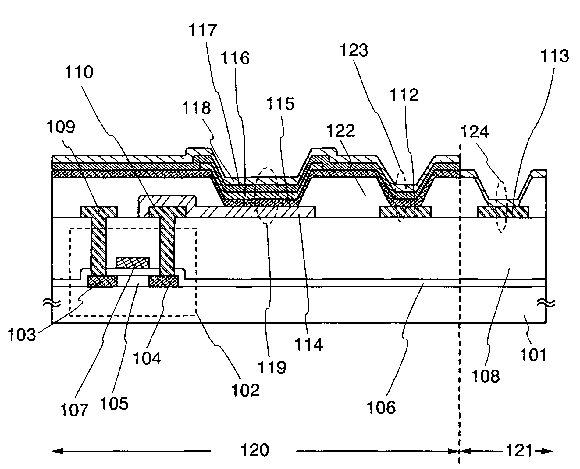
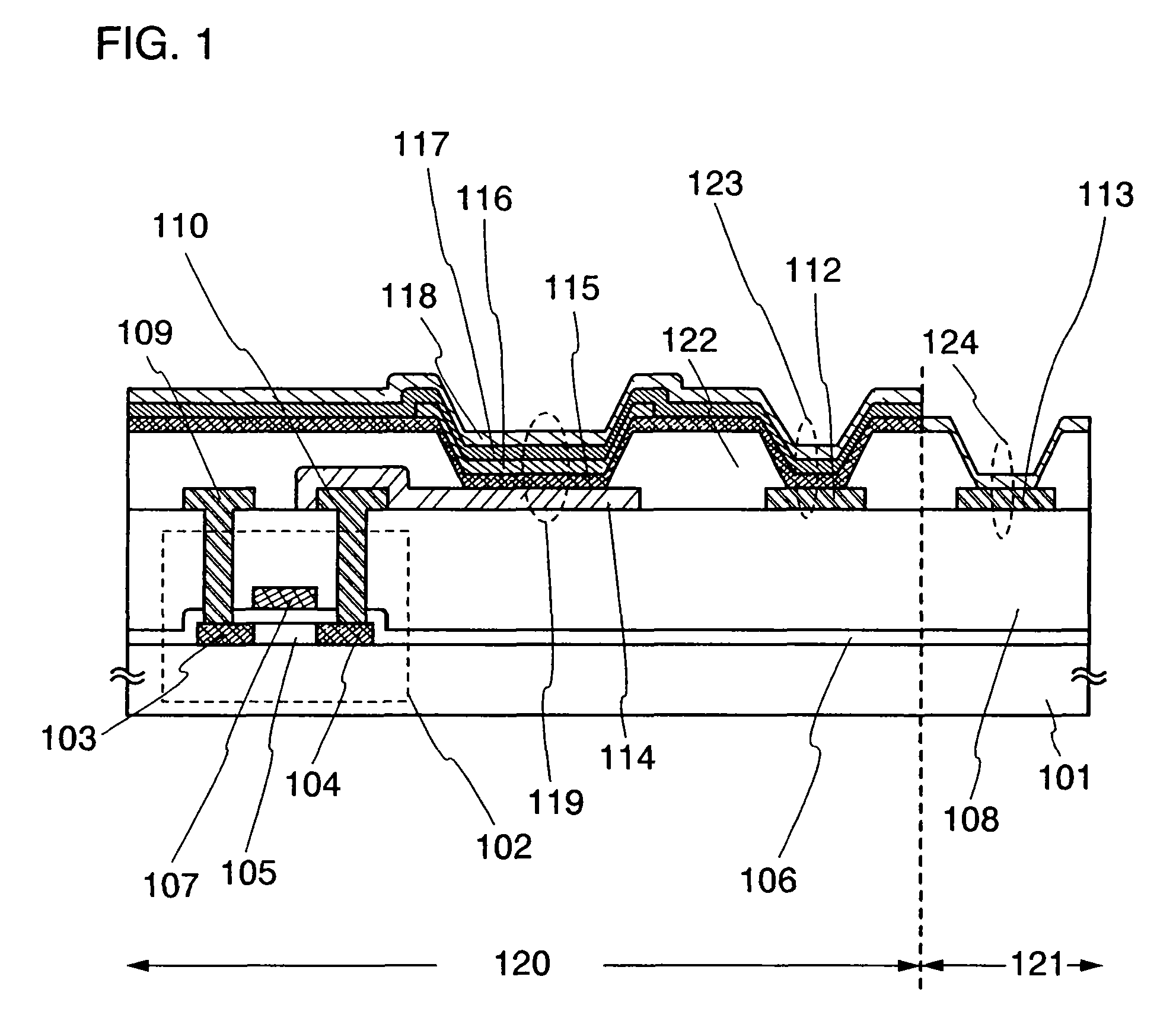
[0045]In this Embodiment Mode 1, an active matrix light emitting display panel which can be used for a light emitting device of the invention will be described, with reference to FIG. 1. In this embodiment, a light emitting element comprising a pair of electrodes is electrically connected to the TFT. One electrode of the pair of electrode (the second electrode) is not directly connected to the TFT. This second electrode is electrically connected not only to an auxiliary wiring formed in a peripheral portion but also to an auxiliary wiring formed in a pixel portion.

[0046]In FIG. 1, in a pixel portion 120 over a substrate 101, a thin film transistor (TFT) is formed. Here, the TFT formed in the pixel portion 120 and electrically connected to a light emitting element 119 is referred to as a current controlling TFT 102.

[0047]In FIG. 1, the current controlling TFT 102 is a top gate type, which includes a source region 103, a drain region 104, a channel forming region 105, a gate electrode...

embodiment mode 2

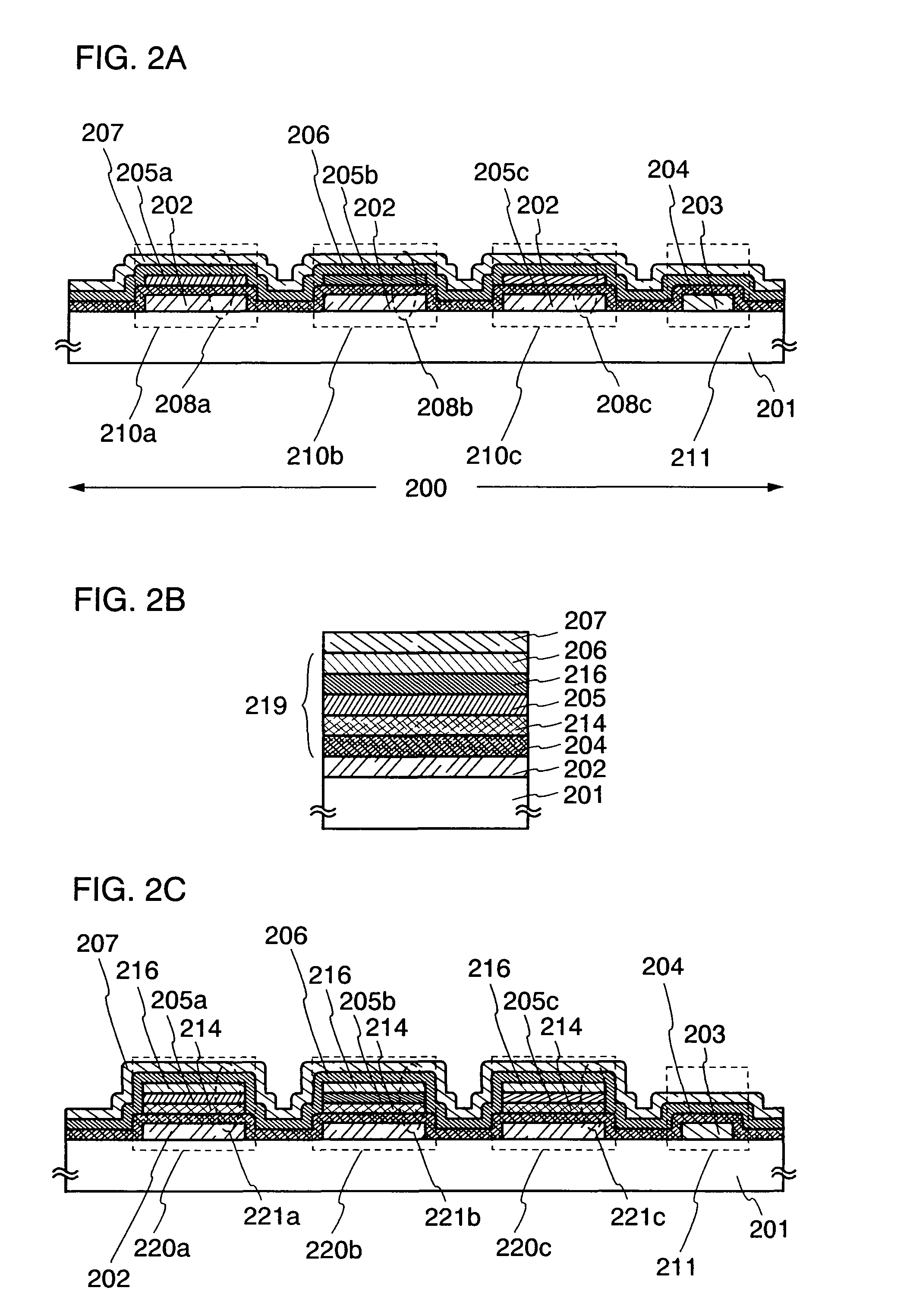
[0071]In this embodiment mode, an example structure of light emitting elements and a connection portion in a pixel portion 200 of a light emitting display panel will be described with reference to cross-sectional views of FIGS. 2A to 2C. It is to be noted that the description of the TFT (the current controlling TFT, a switching TFT or the like), the interlayer insulating film, the insulator, and the like formed in the pixel portion over the substrate as described in FIG. 1 is omitted herein, in order to simplify, the description of a structure of the light emitting element and the connection portion formed in each pixel.

[0072]As shown in FIG. 2A, a plurality of pixels (a pixel R (210a) which emits red light, a pixel G (210b) which emits green light, and a pixel B (210c) which emits blue light), and a connection portion 211 are formed over a substrate 201.

[0073]The pixel R (210a) has a light emitting element R (208a) in which a first electrode 202, a first buffer layer 204, a light e...

embodiment mode 3

[0081]In this embodiment mode, an example structure of light emitting elements and a connection portion in a pixel portion 300 of a light emitting display panel, which is different from the Embodiment Mode 2 will be described, with reference to cross-sectional views of FIGS. 3A and 3B. It is to be noted that the description of the TFT (the current controlling TFT, a switching TFT or the like), the interlayer insulating film, the insulator, and the like formed in the pixel portion over the substrate as described in FIG. 1 is omitted herein, in order to simplify the description of a structure of the light emitting element and the connection portion formed in each pixel.

[0082]As shown in FIG. 3A, a plurality of pixels (a pixel R (310a) which emits red light, a pixel G (310b) which emits green light, and a pixel B (310c) which emits blue light) and a connection portion 311 are formed over a substrate 301.

[0083]The pixel R (310a) has a light emitting element R (308a) in which a first ele...


PUM


Abstract

An active matrix light emitting device of which luminance characteristic does not vary among light emitting elements of respective pixels, and which can be realized even in a high definition display panel is disclosed. In the light emitting device, a light emitting material is interposed between a first electrode and a second electrode electrically connected to an auxiliary wiring, not only in a peripheral portion but also in a pixel portion. A layer containing the light emitting material comprises a first buffer layer, a light emitting layer, and a second buffer layer. In the pixel portion, either one or both of the first and the second buffer layer are interposed between the auxiliary wiring and the second electrode where the second electrode and the auxiliary wiring are electrically connected.

Description

BACKGROUND OF THE INVENTION[0001]1. Field of the Invention[0002]The present invention relates to a light emitting device having a light emitting element, and a manufacturing method thereof.[0003]2. Description of the Related Art[0004]A light emitting element having a light emitting material interposed between a pair of electrodes (an anode and a cathode), which is thin, light, and capable of fast response, is expected to be applied to a next-generation flat panel display. Furthermore, a light-emitting device in which light emitting elements are arranged in a matrix is said to be superior to a conventional liquid crystal display device in that it has wider view angle and higher visibility.[0005]A simple matrix mode and an active matrix mode can be given as driving methods of a light emitting device, and the active matrix mode using an active element such as a thin film transistor (TFT) is adopted in many cases for high-definition panels (for example, a panel having more pixels than Q...

Claims


Application Information

Patent Timeline
Patent Type & Authority Patents(United States)
IPC IPC(8): H01L29/201
CPCH01L27/3276H01L51/5228H01L51/5076H01L51/506H10K59/131H10K50/155H10K50/165H10K50/824
Inventor NAKAMURA, YASUOSHIBATA, NORIKO
Owner SEMICON ENERGY LAB CO LTD
Why Eureka
Try Eureka