
Transmission and reflection dual operational mode light processing device

Inactive Publication Date: 2011-08-09
RUAN JU AI
View PDF6 Cites 10 Cited by
  • Summary
  • Abstract
  • Description
  • Claims
  • Application Information

AI Technical Summary

Benefits of technology

[0005]Aspects of the present invention facilitate the efficient utilization of light in image display devices. One aspect of the invention includes forming a light separator, which directs light uniformly illuminated on a surface (generally the backside or entrance surface of a display panel, the first surface) into individual pixels on the viewing surface (generally called the front side surface, the second surface), and to condense the light within each pixel to exit only through small exit grooves, so that light spreads over only a small fraction of the pixel space. A large portion of the viewing surface is thus free for building or placing light switching structures and integrated circuits (ICs). The ICs are used to control the position of the light switches (concurrently called light shutters) which in turn to control the final path of light in each pixel, either to let the light pass through to viewer or to block it off.
[0006]Another embodiment of the invention is forming micro-electro-mechanical (MEM) light switches (shutters) to control the final path of light in each pixel, either let light to pass through to viewer or block it off from reaching to viewer, depending on the position of the shutters. The function of the light shutter is similar to that of liquid crystal in LCD. But unlike LCD, polarizer, a material that reduces the passage of ordinary un-polarized light (usually reduces by fifty percent) is eliminated from the new device. And unlike plasma display (PD), this device allows the use of efficient external light sources instead of internal plasma discharge inside each pixel, which is generally less energy efficient. Thus power consumption of the new display device is reduced compared to both LCD and PD for similar display outputs (similar panel size and brightness).
[0007]Another embodiment of the invention is forming light shutters with specific characteristics: that they are easy to address electrically (to be able to turn ON and OFF using relatively low voltages); that they are effective in blocking light when turned OFF and in passing the light through to viewer when turned ON; and that they have small moment of inertia with fast response speed. These characteristics are obtained by building dual layer shutters. The primary function of the first layer of the dual layer shutters is to provide effective electrostatic interaction with addressing electrodes, so that low voltage addressing of the shutter (rotate the shutters to their specific landing positions) is possible. This layer of shutter is placed sufficiently close to the addressing electrodes and is free to rotate in both directions around its axis of rotation (hinge) within certain range of angles. This layer of shutter generally lands on one of its two stable positions: ON or OFF position. Hinges are attached to light separator through hinge posts (also called via). The second shutter layer is to provide light switching action. As such, its position is in alignment with the light exiting grooves, i.e., it is placed directly above the light exiting grooves in the light separator. It covers the space above the light exit grooves but not everywhere else. This reduces the total mass of the shutter. In addition, the second shutter layer is formed such that its center of mass is close to its hinges so that the moment of inertia of the entire shutter is minimized. In some applications, a second auxiliary shutter within each pixel comprising only the first shutter layer is used. This auxiliary shutter provides some added light switching ability to the second shutter layer (top shutter layer) of the first shutter, allowing the first shutter to be made slightly smaller than would be needed if the auxiliary shutter is not used.
[0008]According to another aspect of the invention, a method of making view angle adjusters on top of the light separator is provided. The view angle adjusters are used to control the amount of light reflected by the second shutter layer in each pixel into different angles, and are built using the same process steps the shutters are made, with no extra manufacturing process steps / costs.
[0011]According to another aspect of the invention, micro-spherical balls are used as spacers for attaching a protective screen (display screen) to the light modulator to cover and protect the MEM structure (light shutters). The micro-spherical balls are placed to the light modulator through self-aligned structures built in the light modulator. The protective screen is made in black color in all area except where light exits from (light exit grooves for each pixel) to substantially increase the contrast ratio of the new display device. In special cases where the new device is operated in reflective mode, the protective screen has additional light entrance windows for each pixel to let ambient light to enter into the modulator.

Problems solved by technology

And unlike plasma display (PD), this device allows the use of efficient external light sources instead of internal plasma discharge inside each pixel, which is generally less energy efficient.

Method used


Image

  • Transmission and reflection dual operational mode light processing device
  • Transmission and reflection dual operational mode light processing device
  • Transmission and reflection dual operational mode light processing device

Examples


Embodiment Construction

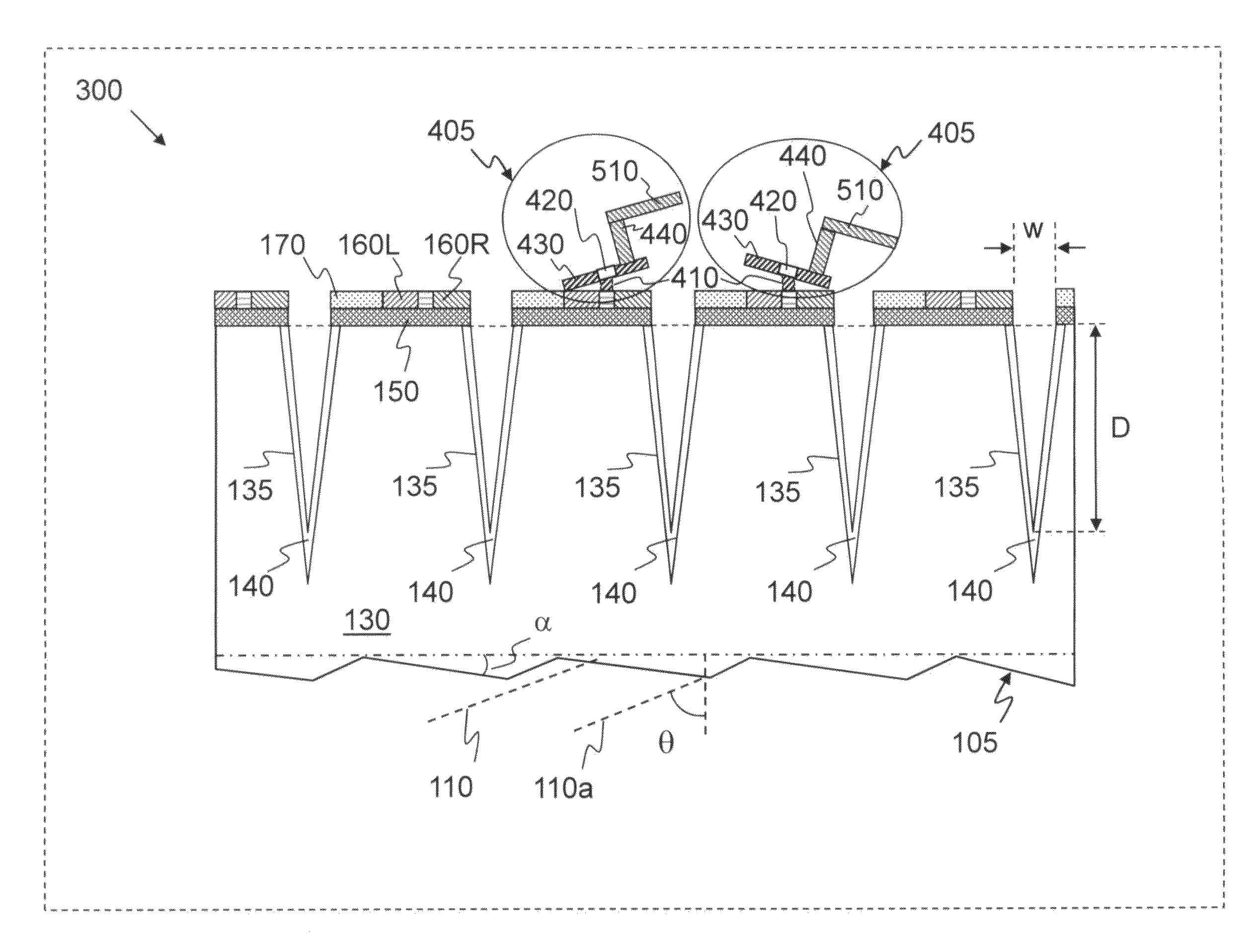
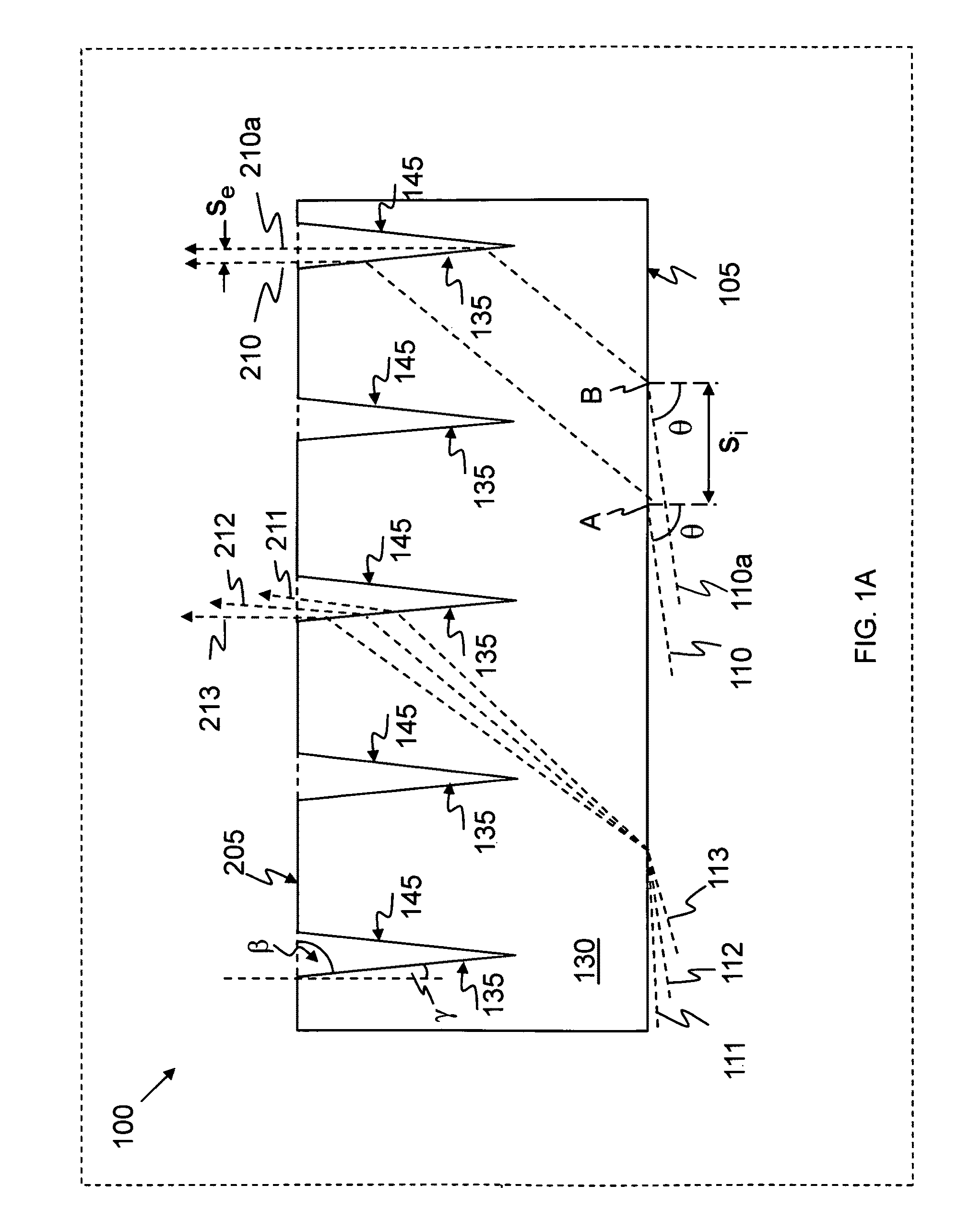
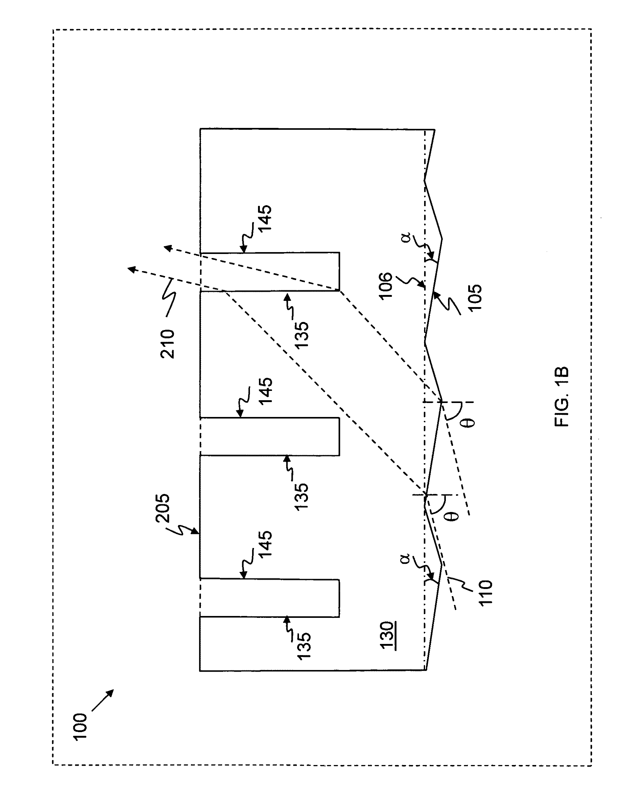
[0033]A new type of display device is created according to the present invention. This new display device is expected to be much more energy efficient than existing ones such as LCD and PD. The new device can also be created using transparent plastic materials as the primary building material for its display panel, making it much more flexible than LCD and PD.

[0034]One aspect of the invention is to use micro-electro-mechanical shutters to control the path of light in a display device, such as but not limited to, backside illuminated flat panel display device. Light under the shutters is let pass through to viewer without much loss when shutters open up the paths (turned “ON”) for light to go through, or is blocked off completely when shutters cut off the paths of the light (turned “OFF”) to prevent the light from reaching to viewers.

[0035]It is obvious that the micro-electro-mechanical shutters occupy a large portion of planar space of a display panel. This would ordinarily block of...


PUM


Abstract

A spatial light modulator suitable for flat panel displays and methods of making the modulators are disclosed. The light modulator comprises a light separator, integrated circuits (IC), light switches (concurrently called light shutters), and optional color filters. The light separator is used to direct light uniformly illuminated on the incident surface (entrance surface) into individual pixels, and condenses the light within each pixel to a small fraction of pixel space on the viewing surface. ICs and light shutters are used to control color and light intensity at individual pixels. Several novel designs of the light modulator and light shutters are disclosed. Methods of building self-aligned structures for placing micro-spherical ball spacers for attaching protective screens to the light modulator is also disclosed.

Description

RELATED APPLICATIONS[0001]This application claims priority to U.S. Provisional Application No. 61 / 011,376, filed Jan. 17, 2008. The content of the aforementioned application is hereby incorporated by reference in its entirety.TECHNICAL FIELD OF THE INVENTION[0002]This invention is generally directed to spatial light modulators, more particularly but not limited, to flat panel display devices and fabrication thereof.BACKGROUND OF THE INVENTION[0003]Liquid crystal display (LCD) and plasma display (PD) are rapidly replacing cathode-ray-tube (CRT) display due to their substantially reduced panel depth compared to CRT. However, both LCD and PD are relatively inefficient in energy use and inflexible in their physical structure. For example, LCD uses polarizer that reduces light intensity by fifty percent, while PD consumes significantly more power per lumen than LCD. There exist a number of disclosures and publications on using micro-electro-mechanical (MEM) devices for display applicatio...

Claims


Application Information

Patent Timeline
IPC IPC(8): G02B26/00
CPCG02B26/02
Inventor RUAN, JU-AI
Owner RUAN JU AI
Features
  • Generate Ideas
  • Intellectual Property
  • Life Sciences
  • Materials
  • Tech Scout
  • Unparalleled Data Quality
  • Higher Quality Content
  • 60% Fewer Hallucinations
Learn More