Bias generation circuit and voltage controlled oscillator

a bias generation circuit and voltage control technology, applied in oscillators, instruments, semiconductor devices/discharge tubes, etc., can solve the problems of not being able to automatically adjust a bias according to variations in the characteristics of elements, the configuration of the bias generation circuit is comparatively complicated, and the bias generation circuit becomes a major noise source within the overall circui

Inactive Publication Date: 2011-08-16
KK TOSHIBA
View PDF6 Cites 16 Cited by
  • Summary
  • Abstract
  • Description
  • Claims
  • Application Information

AI Technical Summary

Problems solved by technology

However, in a bias generation circuit of a simple configuration that uses only variable resistors, it is not possible to automatically adjust a bias according to variations in the characteristics of elements.
Therefore, in general, a bias generation circuit is configured by a comparatively complicated circuit that uses many elements including transistors.
Thus, because a bias generation circuit has a complicated circuit configuration that includes transistors, in some cases a bias generation circuit becomes a major noise source within the overall circuit.
Due to the influence thereof, flicker noise also mixes with a bias voltage (current) that is generated by a bias generation circuit, and adversely affects the operation of a circuit to which the bias is supplied.
That is, a low-pass filter with a large area is required in order to reduce noise occurring in a bias voltage (current), which leads to an increase in the size of an LSI and an increase in costs.

Method used


Image

  • Bias generation circuit and voltage controlled oscillator
  • Bias generation circuit and voltage controlled oscillator
  • Bias generation circuit and voltage controlled oscillator

Examples


first embodiment

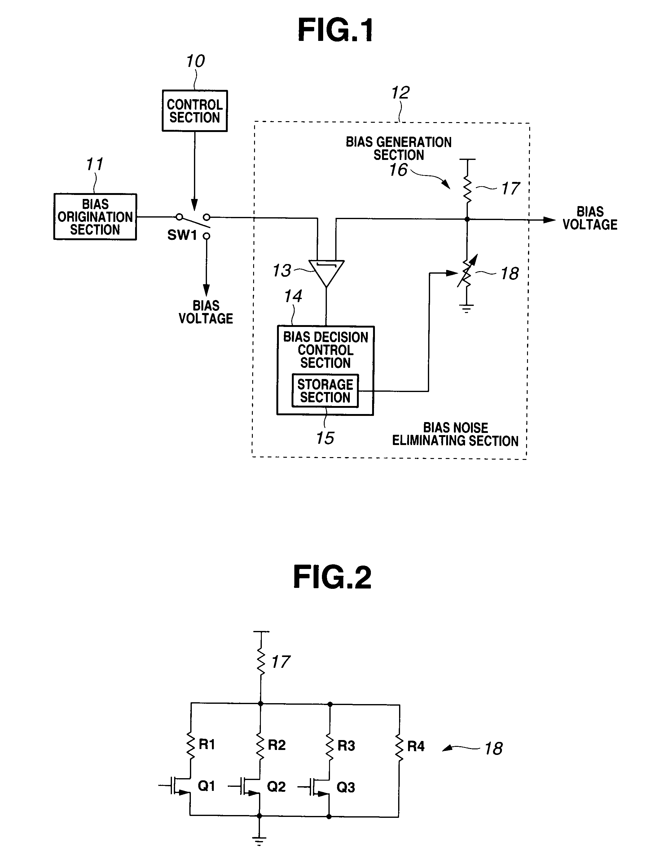
[0021]FIG. 1 is a block diagram that illustrates a bias generation circuit according to the first embodiment of the present invention. In FIG. 1, a bias origination section 11 originates a bias voltage to be supplied to various elements or circuits and the like. The bias origination section 11 originates a bias voltage that is required in order to stably drive elements and circuits and the like in accordance with temperature changes, power supply voltage fluctuations, and variations in manufacturing of the elements. For example, a case is assumed in which a bias voltage from the bias origination section 11 is utilized as a gate bias voltage of a transistor (not shown). In this case, for example, the bias origination section 11 is configured to be capable of originating a bias voltage such that a transconductance (gm) of a transistor to which a bias voltage is supplied is constant, irrespective of fluctuations in the power supply voltage, temperature changes, manufacturing variations...

second embodiment

[0059]FIG. 5 is a circuit diagram that illustrates a second embodiment of the present invention. Components shown in FIG. 5 that are the same as the components in FIG. 1 are denoted by the same reference numerals, and a description of these components is omitted hereunder.

[0060]The present embodiment differs from the first embodiment in that a resistive divider section 16a is adopted instead of the bias generation section 16, and an output section 21 is added. The resistive divider section 16a has the same configuration as that of the bias generation section 16. The output section 21 is composed by a resistor Ra and a variable resistor section RV that are connected in series between a power source terminal and a reference potential point. The variable resistor section RV is configured so that a resistance value thereof is decided based on bias decision data from the bias decision control section 14. For example, the output section 21 is configured in the same manner as the bias gene...

third embodiment

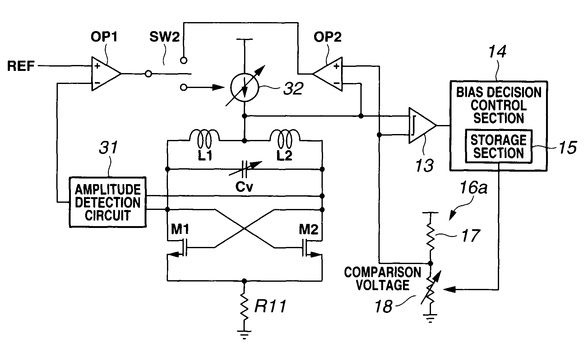
[0068]FIG. 6 is a circuit diagram that illustrates a third embodiment of the present invention. FIG. 6 shows a voltage controlled oscillator that is suitable for large scale integration. Components shown in FIG. 6 that are the same as the components in FIG. 2 are denoted by the same reference numerals, and a description of these components is omitted hereunder.

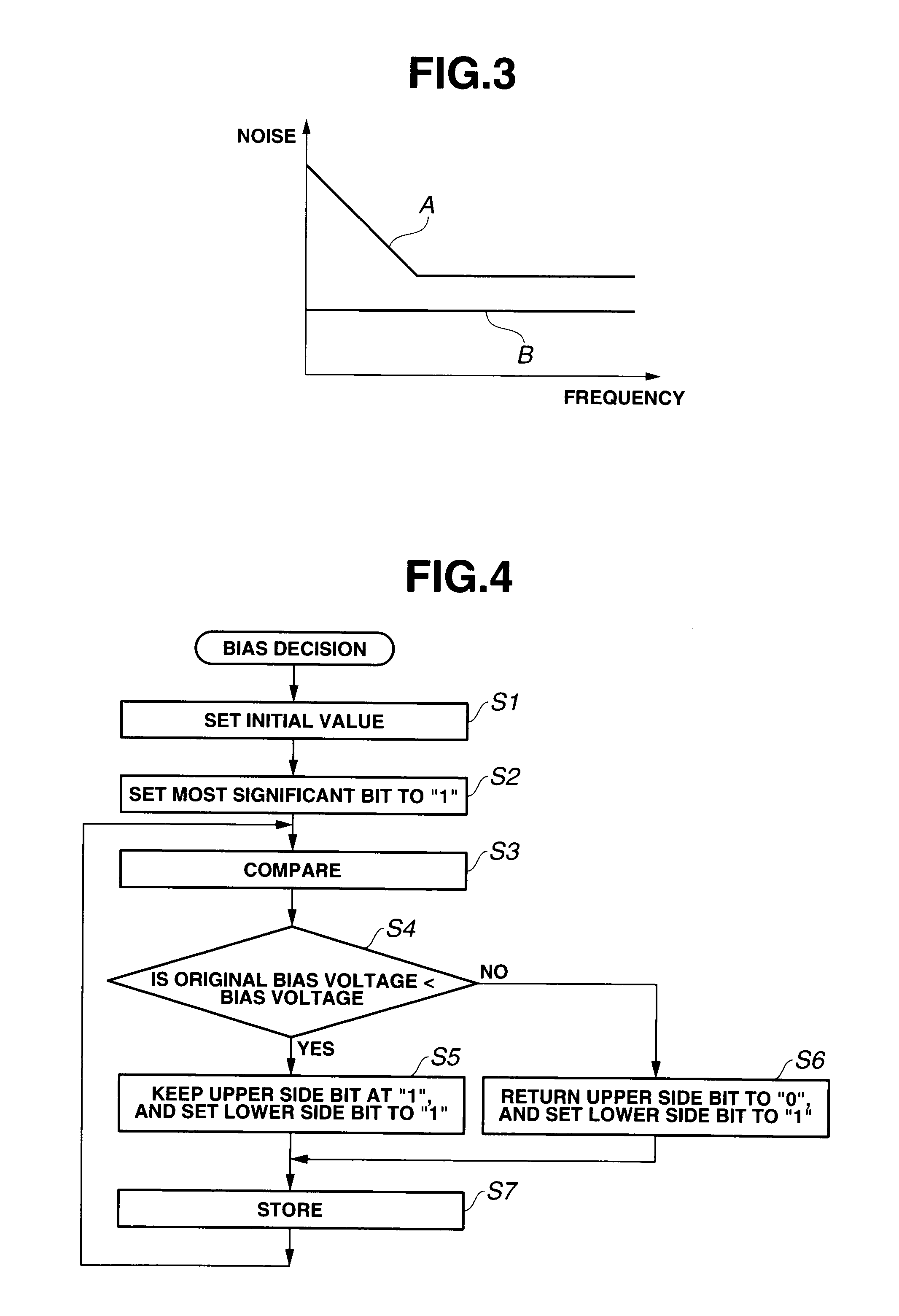
[0069]In a voltage controlled oscillator, if a bias current is merely controlled to a desired value, the oscillation amplitude will change each time the oscillation frequency changes. With regard to this problem, Japanese Patent Application Laid-Open Publication No. 2006-197571 discloses technology that makes an oscillation amplitude constant irrespective of the oscillation frequency.

[0070]However, in the invention of the aforementioned publication also, low-frequency noise mixes with a bias current as the result of flicker noise occurring in an oscillation transistor and the noise of a reference voltage (REF) for bias current...


PUM


Abstract

This invention includes a bias origination section configured to originate an original bias voltage; a comparison section configured to compare the original bias voltage and a comparison voltage, and output a comparison result; a resistive divider section composed by a resistance circuit including a variable resistor section having a resistor and a switch, and configured to generate the comparison voltage; a bias decision control section configured to determine bias decision data for controlling a resistance value of the variable resistor section so as to bring the comparison voltage close to the original bias voltage, based on a comparison result of the comparison section; and a storage section configured to hold the bias decision data and also output the comparison voltage as a bias voltage by controlling a resistance value of the variable resistor section based on the held bias decision data, thereby generating a low-noise bias with a small area.

Description

CROSS-REFERENCE TO RELATED APPLICATION[0001]This application is based upon and claims the benefit of priority from the prior Japanese Patent Application No. 2009-65289 filed in Japan on Mar. 17, 2009; the entire contents of which are incorporated herein by reference.BACKGROUND OF THE INVENTION[0002]1. Field of the Invention[0003]The present invention relates to a bias generation circuit and a voltage controlled oscillator that are suitable for a large-scale integrated circuit for radio communication.[0004]2. Description of Related Art[0005]Conventionally, in an LSI for radio communication, various bias voltages (or currents) are supplied to the circuit. For example, in order to decide the operating point of a transistor, a bias voltage is applied to a gate of the transistor. Further, for example, a bias current is supplied by a current source to a common source of transistors that configure a differential amplifier. A bias generation circuit that generates this kind of bias can be c...

Claims


Application Information

Patent Timeline
Patent Type & Authority Patents(United States)
IPC IPC(8): H03L1/00
CPCH03B5/1228H03B5/1215H03B5/1243H03B5/1278
Inventor MIYASHITA, DAISUKE
Owner KK TOSHIBA
Why Eureka
Try Eureka