Semiconductor device having wiring line and manufacturing method thereof

a technology of semiconductor devices and wiring lines, which is applied in the direction of semiconductor devices, semiconductor/solid-state device details, electrical apparatus, etc., can solve the problems of limiting the miniaturization of semiconductor constructs and being unable to adapt to an increase in the number of columnar electrodes, and achieve the effect of further miniaturization

Inactive Publication Date: 2011-08-23
TERAMIKROS INC
View PDF29 Cites 126 Cited by
  • Summary
  • Abstract
  • Description
  • Claims
  • Application Information

AI Technical Summary

Benefits of technology

[0010]a semiconductor construct having a semiconductor substrate and an external connection electrode provided on the semiconductor substrate;

Problems solved by technology

Therefore, the problem is that there is a limit to the miniaturization of the semiconductor construct and it is impossible to adapt to an increase in the number of columnar electrodes.

Method used


Image

  • Semiconductor device having wiring line and manufacturing method thereof
  • Semiconductor device having wiring line and manufacturing method thereof
  • Semiconductor device having wiring line and manufacturing method thereof

Examples


first embodiment

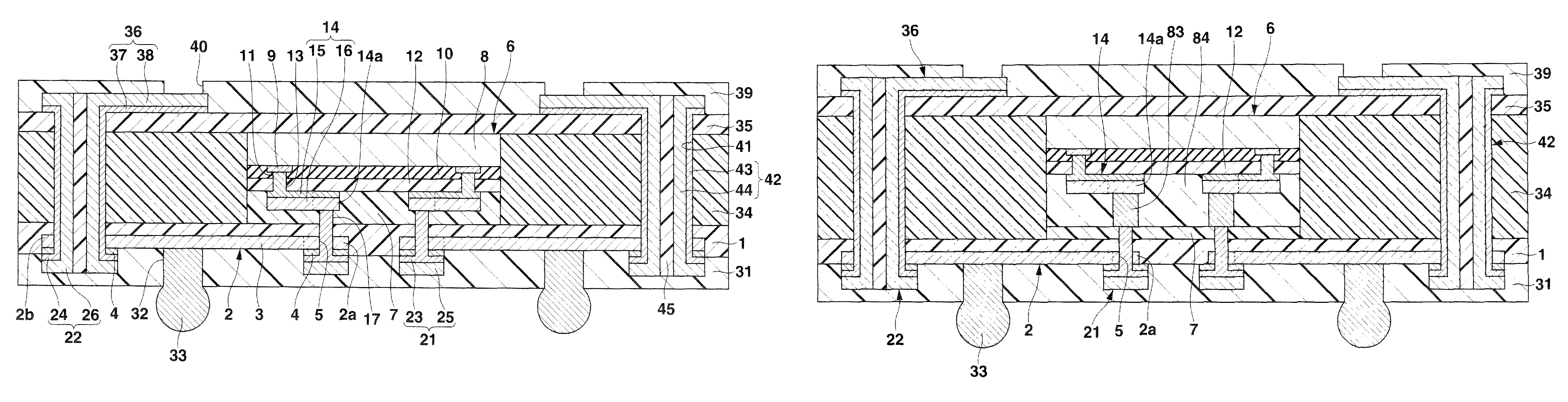
[0050]FIG. 1 shows a sectional view of a semiconductor device as a first embodiment of this invention. This semiconductor device comprises a planar square lower insulating film 1 made of, for example, an epoxy resin, a polyimide resin, or an epoxy resin having a glass cloth base material. A lower wiring line (laminated wiring line) 2 is embedded in the lower side of the lower insulating film 1. The lower wiring line 2 has a structure in which a foundation metal layer 4 made of nickel is provided on the lower surfaces of both ends of an upper metal layer 3 made of copper. At both ends of the double-layer structure of the lower wiring line 2, there are a connection pad portion 2a located in the center of the lower surface of the lower insulating film (insulating film) 1, and a connection pad portion 2b located in the peripheral part of the lower surface of the lower insulating film 1.

[0051]The lower surface of the foundation metal layer (mask metal layer) 4 of the connection pad porti...

second embodiment

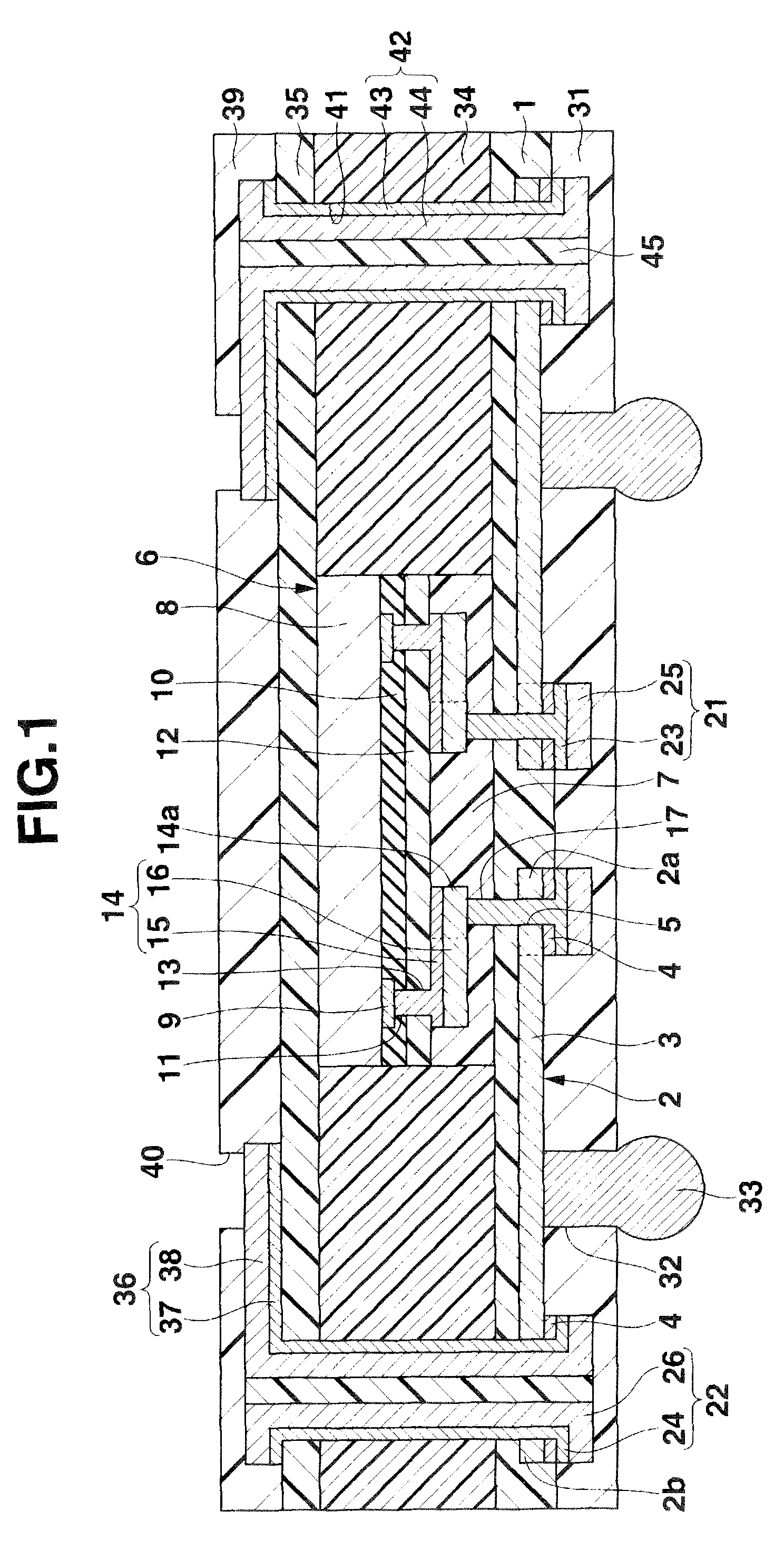
[0093]FIG. 13 shows a sectional view of a semiconductor device as a second embodiment of this invention. This semiconductor device is different from the semiconductor device shown in FIG. 1 in that the outside diameter of an upper metal layer 3 of a connection pad portion 2a of a lower wiring line 2 is substantially equal to the diameter of a connection pad portion 14a of a wiring line 14 of a semiconductor construct 8 and in that a foundation metal layer 4 of the connection pad portion 2a of the lower wiring line 2 is slightly larger than the outside diameter of the upper metal layer 3.

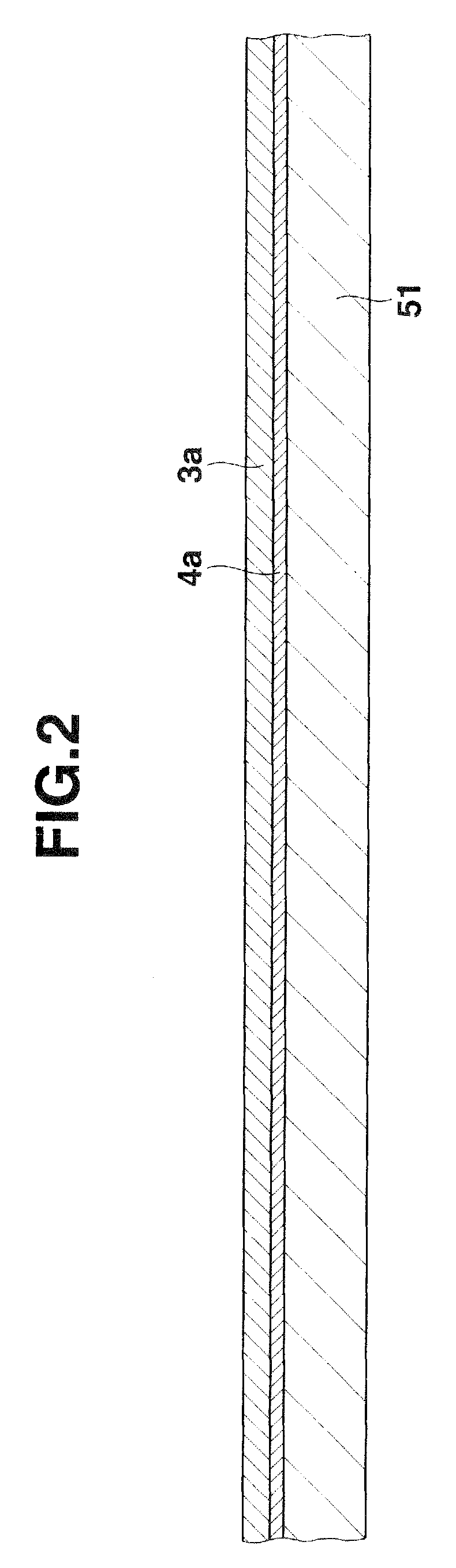
[0094]Next, one example of a method of manufacturing this semiconductor device is described. First, a unit shown in FIG. 2 is prepared. Then, as shown in FIG. 14, an opening 5 is formed in a lower wiring line upper metal layer forming layer 3a and a lower wiring line foundation metal layer forming layer (mask metal layer forming layer) 4a by the photolithographic method. Further, the lower wiring lin...

third embodiment

[0110]FIG. 24 shows a sectional view of a semiconductor device as a third embodiment of this invention. This semiconductor device is greatly different from the semiconductor device shown in FIG. 13 in that both a lower wiring line and an upper wiring line are formed to have a double-layer wiring structure by a build-up method. That is, a second lower insulating film 1B made of the same material as a first lower insulating film 1A is provided on the lower surface of a first lower wiring line 2A including first and second connection pad portions 21, 22 and on the lower surface of the first lower insulating film 1A.

[0111]One end of a second lower wiring line 2B provided on the lower surface of the second lower insulating film 1B is connected to the connection pad portion of the first lower wiring line 2A via an opening 61 provided in the second lower insulating film 1B. A lower overcoat film 31 is provided on the lower surface of the second lower insulating film 1B including the second...


PUM


Abstract

On the lower surface of a semiconductor construct having an external connection electrode, there are formed an insulating film having a planar size greater than that of the semiconductor construct, and a metal layer and a mask metal layer having a connection pad portion in which a first opening corresponding to the external connection electrode is formed. A laser beam is applied using the mask metal layer as a mask, and a second opening is thereby formed in a part of the insulating film corresponding to the external connection electrode. Then, a connection conductor is formed to connect a wiring line to the external connection electrode via the second opening of the insulating film.

Description

CROSS-REFERENCE TO RELATED APPLICATIONS[0001]This application is based upon and claims the benefit of priority from prior Japanese Patent Application No. 2008-020692, filed Jan. 31, 2008, the entire contents of which are incorporated herein by reference.BACKGROUND OF THE INVENTION[0002]1. Field of the Invention[0003]This invention relates to a semiconductor device having a wiring line and a manufacturing method thereof.[0004]2. Description of the Related Art[0005]In a method employed to increase the packaging density of a semiconductor device, a semiconductor construct called a chip size package (CSP) is provided on a base plate having a planar size greater than that of the semiconductor construct. Jpn. Pat. Appln. KOKAI Publication No. 2004-71998 discloses the structure of such a semiconductor device and a manufacturing method thereof. In the semiconductor device disclosed in this prior literature, an insulating layer is provided on the base plate around the semiconductor construct...

Claims


Application Information

Patent Timeline
Patent Type & Authority Patents(United States)
IPC IPC(8): H01L23/522
CPCH01L23/49816H01L24/18H01L24/82H01L24/83H01L25/105H01L24/29H01L23/5389H01L2224/0401H01L2224/18H01L2224/82039H01L2224/83191H01L2224/8385H01L2224/92144H01L2924/01002H01L2924/01005H01L2924/01013H01L2924/01015H01L2924/01029H01L2924/01047H01L2924/01078H01L2924/01082H01L2924/07802H01L2924/14H01L2924/15311H01L2224/2919H01L2924/01006H01L2924/01033H01L2924/014H01L2924/0665H01L2224/92244H01L2224/73267H01L2224/32225H01L2224/12105H01L2224/04105H01L2225/1058H01L2924/3511H01L2225/1035H01L2924/00H01L2924/3512H01L21/568H01L24/19H01L2924/181H01L23/12H01L23/52
Inventor JOBETTO, HIROYASU
Owner TERAMIKROS INC
Why Eureka
Try Eureka