Supercharge Your Innovation With Domain-Expert AI Agents!

Method of forming a seam-free tungsten plug

a technology of seam-free tungsten and tungsten plug, which is applied in the direction of basic electric elements, electrical apparatus, semiconductor devices, etc., can solve the problem of difficult control of the resistance of the plug

Active Publication Date: 2011-10-11
SAMSUNG ELECTRONICS CO LTD
View PDF10 Cites 22 Cited by
  • Summary
  • Abstract
  • Description
  • Claims
  • Application Information

AI Technical Summary

Benefits of technology

The patent text describes a plug and a method of forming a plug for a phase changeable memory device. The plug includes a first insulating interlayer, a tungsten pattern, and a tungsten oxide pattern. The tungsten oxide pattern has a level face and may protrude over the first insulating interlayer. A barrier metal layer may be formed on the sidewall of the contact hole. The tungsten pattern may be formed by converting the upper portion of the tungsten layer in the contact hole or by re-growing or swelling the tungsten pattern. The plug can be used in a phase changeable memory device, where it is connected to a phase-changeable layer. The technical effects of the patent text include improved stability and reliability of the plug and the phase changeable memory device.

Problems solved by technology

When the seam or the void is exposed, it may be difficult to control a resistance of the plug.

Method used


Image

  • Method of forming a seam-free tungsten plug
  • Method of forming a seam-free tungsten plug
  • Method of forming a seam-free tungsten plug

Examples


Embodiment Construction

[0030]This application claims priority under 35 USC §119 to Korean Patent Application No. 10-2008-0069700 filed on Jul. 17, 2009 in the Korean Intellectual Property Office (KIPO), the contents of which are herein incorporated by reference in their entirety.

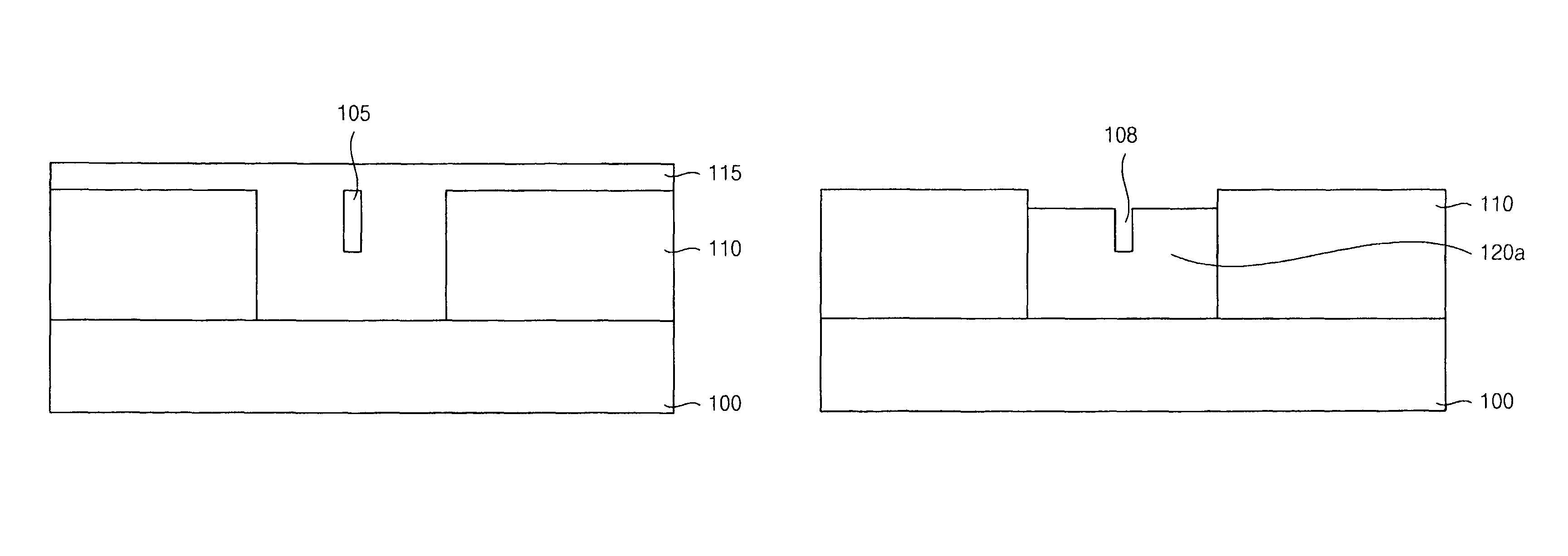
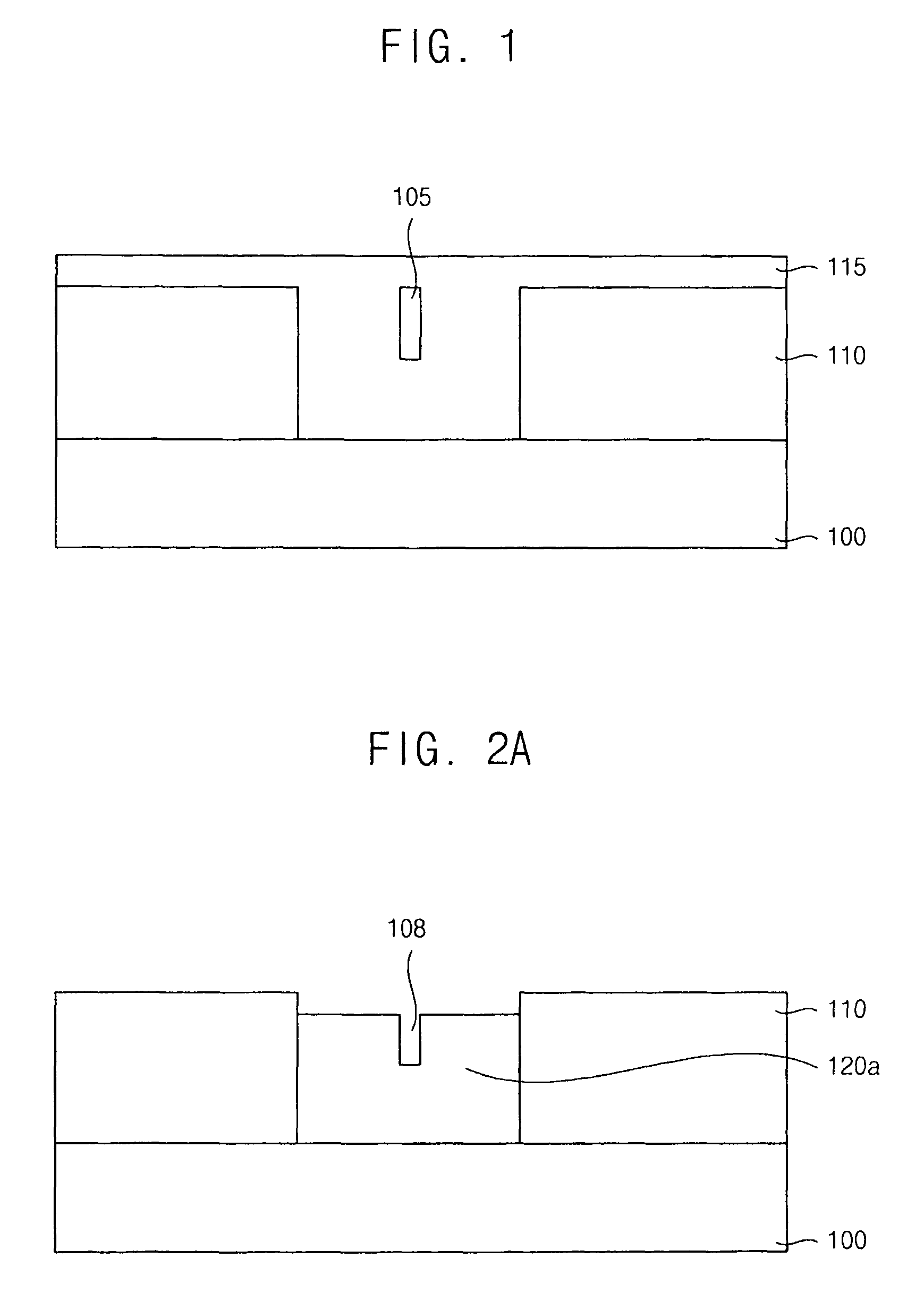
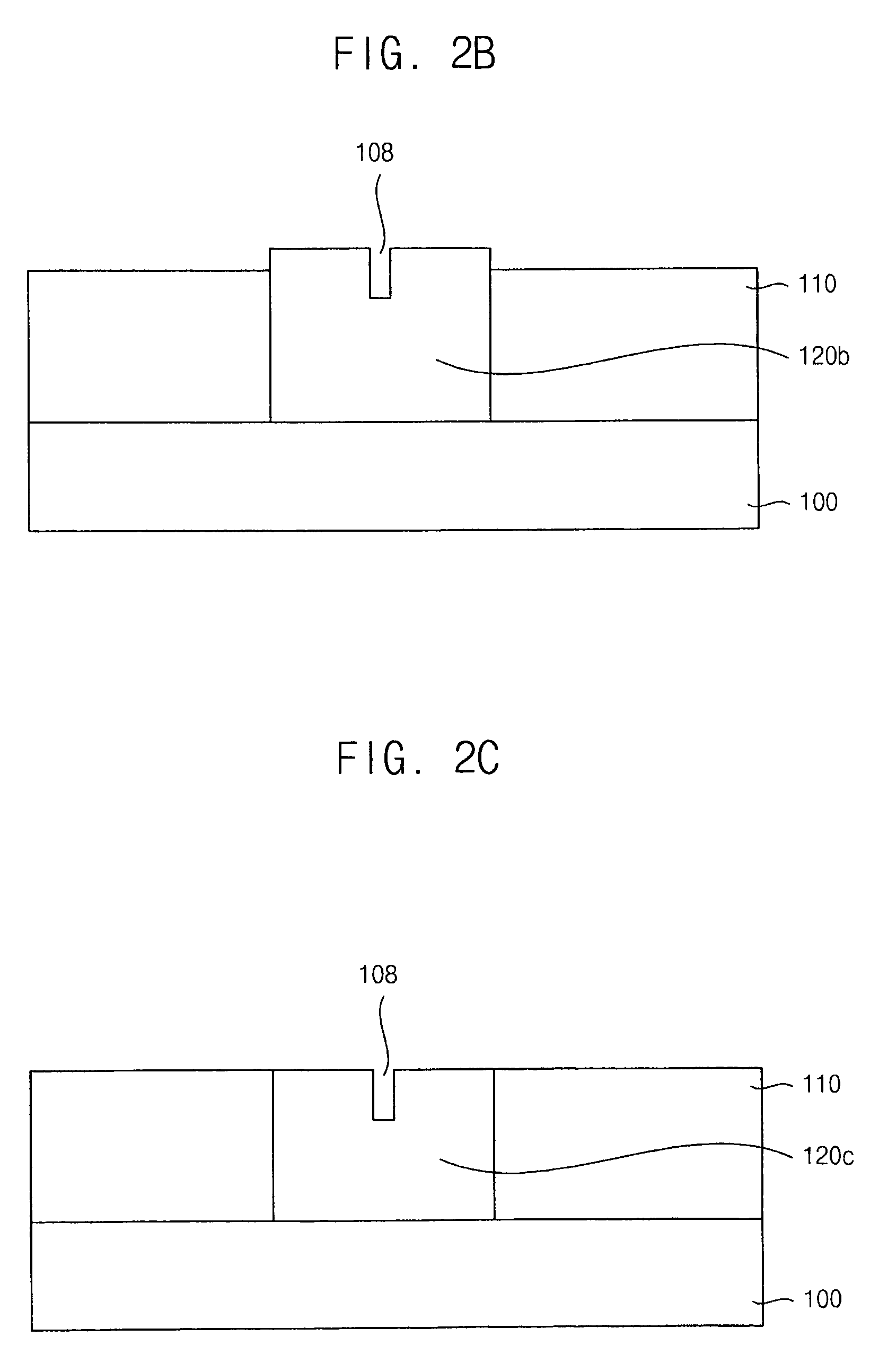
[0031]Various exemplary embodiments will be described more fully hereinafter with reference to the accompanying drawings, in which some exemplary embodiments are illustrated. The present invention may, however, be embodied in many different forms and should not be construed as limited to the exemplary embodiments set forth herein. Rather, these exemplary embodiments are provided so that this description will be thorough and complete, and will fully convey the present invention to those skilled in the art. In the drawings, the sizes and relative sizes of layers and regions may be exaggerated for clarity.

[0032]It will be understood that when an element or layer is referred to as being “on,”“connected to” or “coupled to” another elem...


PUM

PropertyMeasurementUnit
swellingaaaaaaaaaa
poweraaaaaaaaaa
resistanceaaaaaaaaaa

Abstract

A plug comprises a first insulating interlayer, a tungsten pattern and a tungsten oxide pattern. The first insulating interlayer has a contact hole formed therethrough on a substrate. The tungsten pattern is formed in the contact hole. The tungsten pattern has a top surface lower than an upper face of the first insulating interlayer. The tungsten oxide pattern is formed in the contact hole and on the tungsten pattern. The tungsten oxide pattern has a level face.

Description

RELATED APPLICATION[0001]This application claims priority under 35 U.S.C. 119 to Korean Patent Application No. 10-2008-0069700, filed in the Korean Intellectual Property Office on Jul. 17, 2009, the entire content of which are incorporated herein by reference.BACKGROUND[0002]1. Field[0003]Exemplary embodiments relate to a tungsten plug, a method of forming a tungsten plug and a semiconductor device having a tungsten plug. More particularly, exemplary embodiments relate to a seam-free tungsten plug, a method of forming a seam-free tungsten plug and a semiconductor device having a seam-free tungsten plug.[0004]2. Description of the Related Art[0005]A semiconductor memory device may be classified as either a volatile memory device or a non-volatile memory device. The volatile memory device requires power in order to maintain its stored information, unlike the non-volatile memory device which does not require that power be maintained in order to retain its data. Types or volatile memory...

Claims


Application Information

Patent Timeline
Patent Type & Authority Patents(United States)
IPC IPC(8): H01L21/4763
CPCH01L21/76879H01L21/76883H01L21/76888H01L27/24H10B63/20H10N70/231H10N70/8828H10N70/011H10N70/826H01L21/324H01L21/28
Inventor CHOI, SUK-HUNHONG, CHANG-KISON, YOON-HOJUNG, JU-YOUNG
Owner SAMSUNG ELECTRONICS CO LTD
Features
  • R&D
  • Intellectual Property
  • Life Sciences
  • Materials
  • Tech Scout
  • Unparalleled Data Quality
  • Higher Quality Content
  • 60% Fewer Hallucinations
Learn More