
Phase-change memory device

a phase-change memory and page buffer technology, applied in the direction of information storage, static storage, digital storage, etc., can solve the problems of sram having the same drawback, dram having a drawback of being volatile, and sram being disadvantageous in terms of cos

Active Publication Date: 2011-10-25
SK HYNIX INC
View PDF4 Cites 7 Cited by
  • Summary
  • Abstract
  • Description
  • Claims
  • Application Information

AI Technical Summary

Benefits of technology

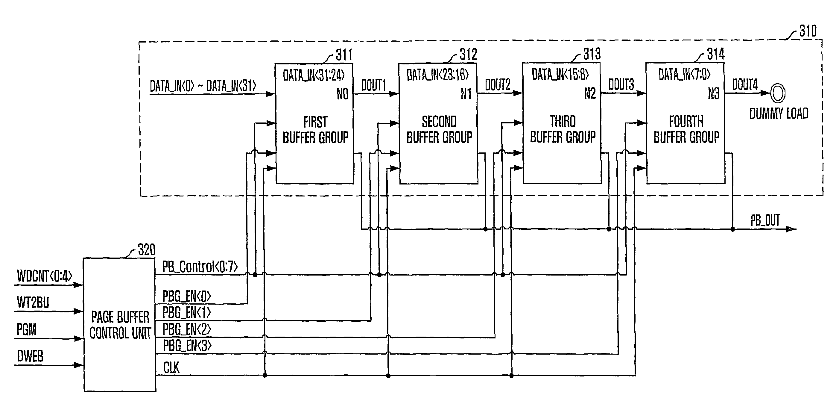
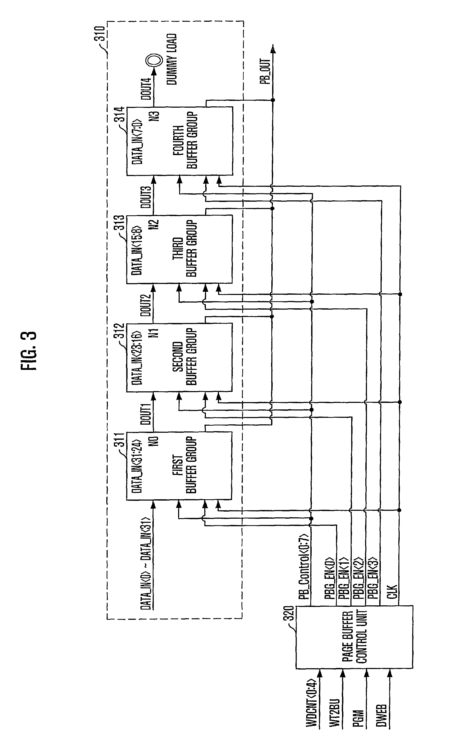
The present invention is about a phase-change memory device that controls a page buffer by up- or down-counting the word count value of a command sequence. This helps to selectively output the stored input data during a buffer program operation. The device includes a page buffer unit and a page buffer control unit that generate the selection signal by counting the word count value. This technology allows for efficient and accurate control of data output from the page buffer, improving the overall performance of the phase-change memory device.

Problems solved by technology

However, the DRAM has a drawback of being a volatile memory.
While a static random access memory (SRAM), used as a cache memory, is capable of random access and is faster than the DRAM in the operating speed, the SRAM has the same drawback.
The SRAM is disadvantageous in terms of cost because it has a memory cell size larger than that of the DRAM.
However, the NAND flash memory has a low operating speed because it is incapable of random access.

Method used


Image

  • Phase-change memory device
  • Phase-change memory device
  • Phase-change memory device

Examples


Embodiment Construction

class="d_n">[0032]FIG. 4 is a diagram illustrating a structure of a buffer group of a page buffer unit of FIG. 3.

[0033]FIG. 5 is a circuit diagram of a buffer of FIG. 4 in accordance with an exemplary embodiment.

[0034]FIG. 6 is a diagram illustrating a structure of a page buffer control unit of FIG. 3.

[0035]FIG. 7 is a diagram illustrating a clock signal generating unit of FIG. 6 in accordance with another embodiment of the present invention.

[0036]FIG. 8 is a diagram illustrating a buffer selection signal PB_CONTROL0:7> and a buffer group selection signal PBG_EN0:3> corresponding to an output signal CNT0:4> of a counter.

[0037]FIG. 9 is a timing diagram illustrating a command sequence for a buffer program operation.

DESCRIPTION OF SPECIFIC EMBODIMENTS

[0038]In order to describe in detail such that those skilled in the art can easily implement the spirit and scope of the present invention, the embodiments of the present invention will be described with reference to the accompanying draw...


PUM


Abstract

A phase-change memory device performs a buffer program operation in response to a buffer program command sequence. The phase-change memory device includes a page buffer unit configured to store a plurality of input data corresponding to a word count value of a buffer program command sequence and selectively output the stored input data in response to a selection signal, and a page buffer control unit configured to generate the selection signal determined by counting a value representing the word count value.

Description

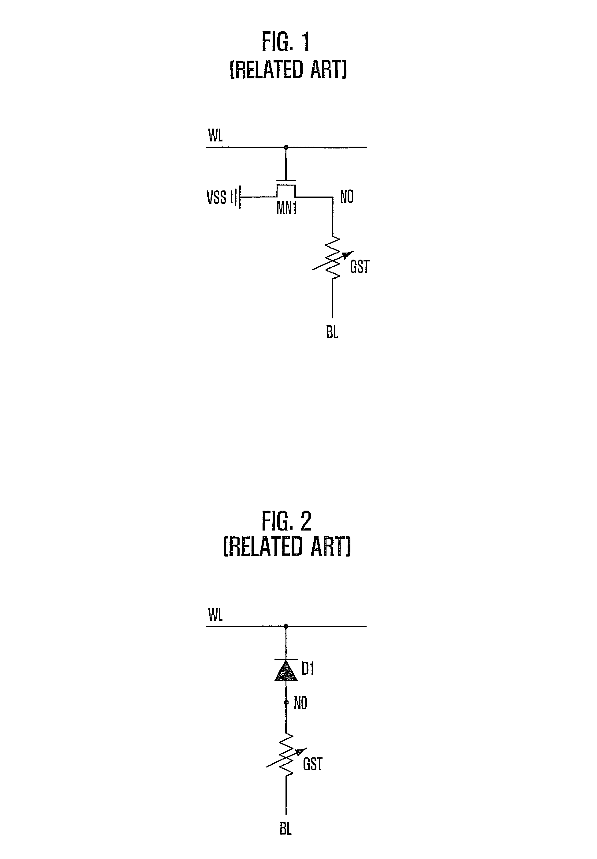
CROSS-REFERENCE TO RELATED APPLICATION[0001]The present invention claims priority of Korean patent application number 10-2008-0126414, filed on Dec. 12, 2008, which is incorporated by reference in its entirety.BACKGROUND OF THE INVENTION[0002]The present invention relates to a semiconductor design technology, and more particularly, to a technology for controlling a page buffer of a phase-change memory device.[0003]Among various memory devices, a dynamic random access memory (DRAM), used as a computer main memory device, is capable of random access and high integration at a low cost. However, the DRAM has a drawback of being a volatile memory. While a static random access memory (SRAM), used as a cache memory, is capable of random access and is faster than the DRAM in the operating speed, the SRAM has the same drawback. The SRAM is disadvantageous in terms of cost because it has a memory cell size larger than that of the DRAM. A NAND flash memory, which is a nonvolatile memory, is ca...

Claims


Application Information

Patent Timeline
Patent Type & Authority Patents(United States)
IPC IPC(8): G11C11/00
CPCG11C8/04G11C8/18G11C13/0004G11C13/0069G11C2013/0085G11C16/10
Inventor EM, HO-SEOK
Owner SK HYNIX INC
Learn More