
Load driving circuit and load driving method

a technology of load driving circuit and load driving method, which is applied in the direction of electrical equipment, instruments, and apparatus without intermediate ac conversion, etc., can solve the problem of significant application limitations, and achieve the effect of reducing power consumption

Active Publication Date: 2011-11-01
SEIKO EPSON CORP
View PDF47 Cites 6 Cited by
  • Summary
  • Abstract
  • Description
  • Claims
  • Application Information

AI Technical Summary

Benefits of technology

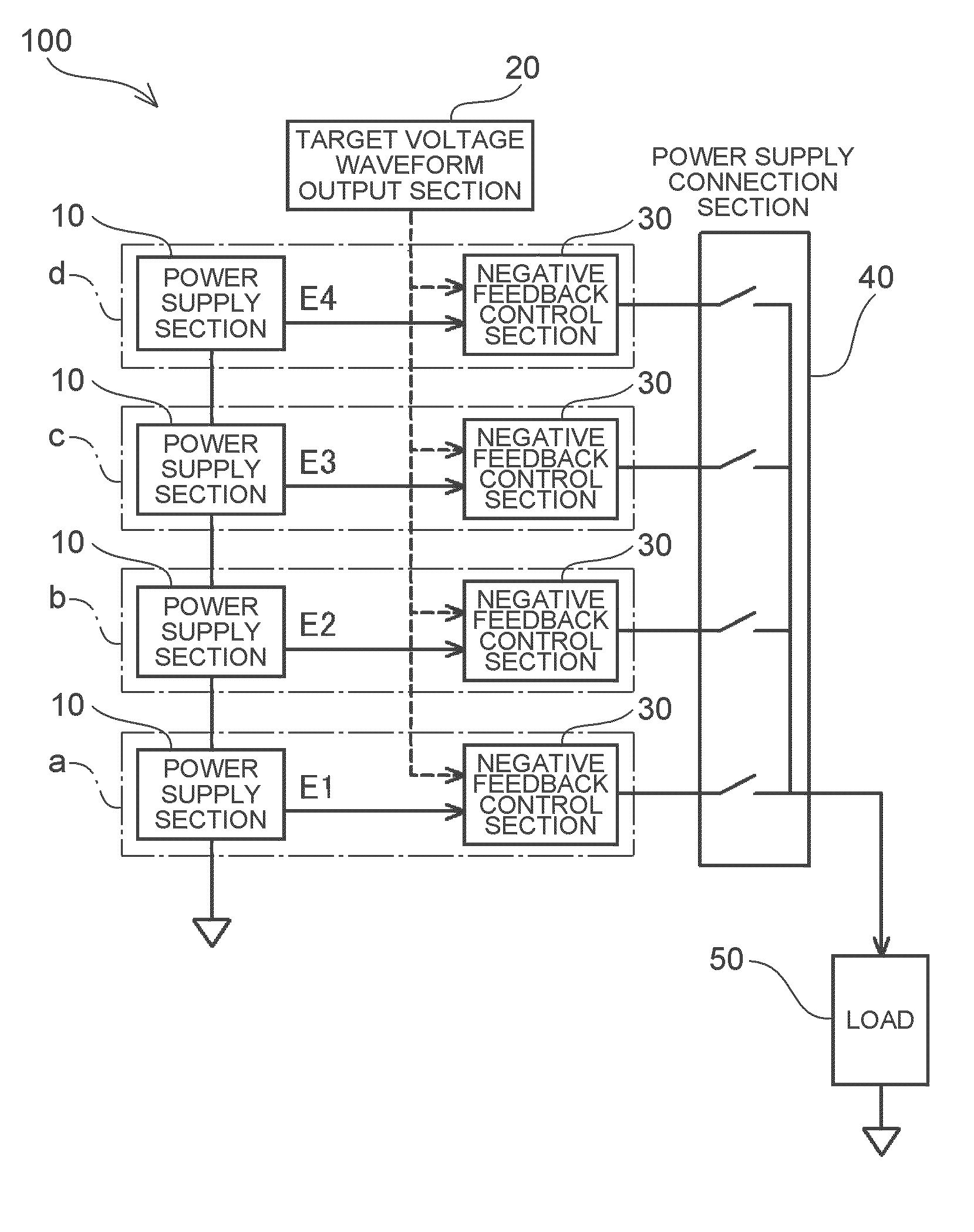
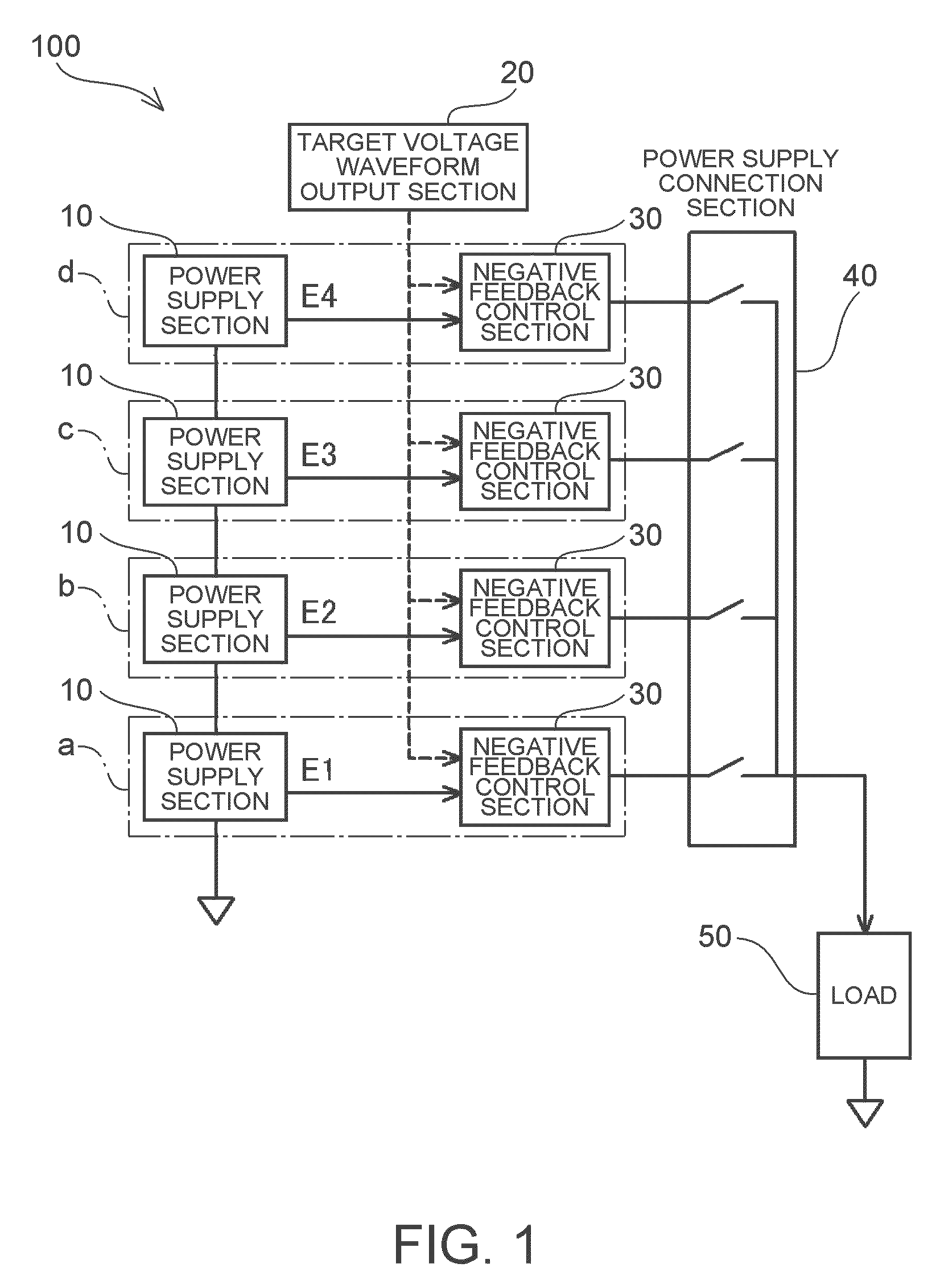
The invention provides a load driving circuit and method that reduces power consumption by using multiple power supply sections with different voltage values and a negative feedback control section to match the voltage value with the desired target waveform. The circuit includes a target voltage waveform output section, power supply sections, negative feedback control sections, and a power supply connection section to select the most suitable power supply section for the load. The negative feedback control section controls the voltage applied to the load to match the target voltage waveform. The circuit can be easily configured using standard components and can be applied to any type of load. Additionally, the circuit includes a variable resistance section to further reduce power consumption. The technical effect of the invention is to provide a load driving circuit with improved power efficiency and reliability.

Problems solved by technology

However, since these proposed technologies are not applicable unless a plurality of loads are driven and the loads are types of load generating counter electromotive force, there arises a problem that the scope of application is significantly limited.

Method used


Image

  • Load driving circuit and load driving method
  • Load driving circuit and load driving method
  • Load driving circuit and load driving method

Examples


first embodiment

B. First Embodiment

B-1. Configuration of Resistive Load Driving Circuit

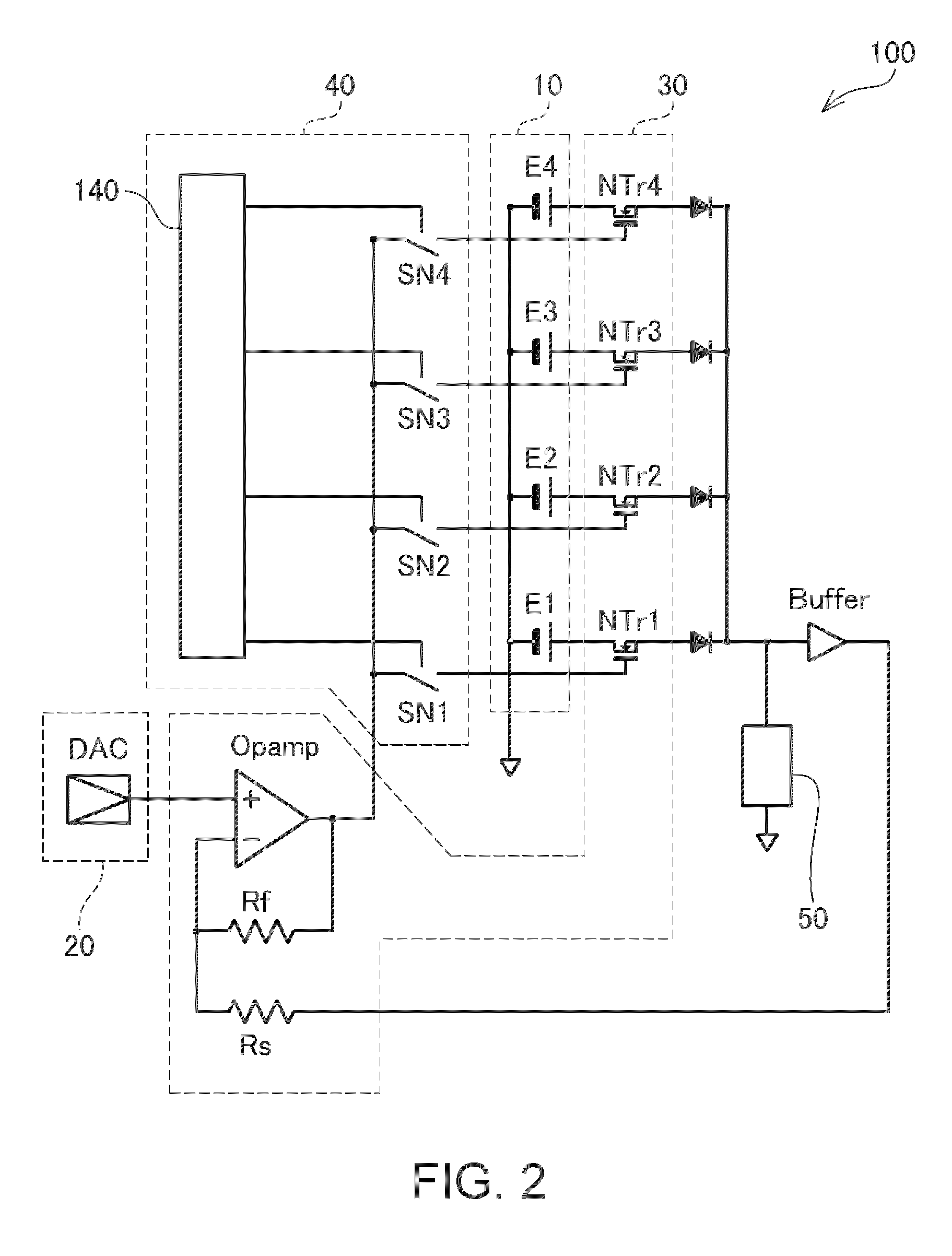
[0052]FIG. 2 is an explanatory diagram exemplifying a configuration of a load driving circuit of a first embodiment. In the example shown in the drawing, there is adopted a configuration in which four power supplies E1 through E4 are disposed, and the electrical power generated by the power supplies E1 through E4 is connected to the load 50 via unipolar NMOS transistors NTr1 through NTr4. It should be noted that as the power supplies E1 through E4, any power supplies such as primary batteries, secondary batteries, mere capacitors, or so-called power supply circuits can be used providing the power supplies generate voltage values different from each other. Further, the transistors NTr1 through NTr4 are not limited to the unipolar transistors, but other types of transistors such as bipolar transistors can also be used therefor. Further, regarding the load 50, although any types of load 50 can be driven, the explana...

second embodiment

C. Second Embodiment

[0076]In the first embodiment described hereinabove, the explanations are presented assuming that the load 50 is a resistive load. However, in the case in which the load 50 is a capacitive load, it becomes possible to more significantly reduce the power consumption. It should be noted here that the capacitive load is a load having a characteristic of storing at least a part of the electrical power supplied thereto, and a load incorporating a piezoelectric element can be cited as a representative example thereof. Further, liquid crystal panels constitutionally cause large parasitic capacitances, and therefore, can also be regarded as capacitive loads. Further, by applying the load driving circuit 100 of the second embodiment to a load composed of a capacitive load and a resistive load coupled in parallel to each other, the power consumption can significantly be reduced. Hereinafter, the load driving circuit 100 of the second embodiment for driving such a capacitiv...

first modified example

D-1. First Modified Example

[0097]In the various types of embodiments described above, the explanations are presented assuming that either of the power supplies E1 through E4 always generates the electrical power with a stable voltage value. However, there exist power supplies, such as capacitors, having the voltage value dropping as the electrical power is supplied, or power supplies, such as secondary batteries, not necessarily generating the electrical power with a stable voltage value. Further, there can be caused the case in which it is difficult to supply the electrical power with a stable voltage value because the electrical power to be supplied to the load 50 is too much in comparison with the capacity of the power supply. In such a case, it is also possible to monitor the value of the voltage generated by each of the power supplies, and switch the switches SN1 through SN4 or the switches SP0 through SP3 so that the power supply generating the voltage with the optimum value i...


PUM


Abstract

A load driving circuit that generates a desired voltage waveform to drive a load includes a target voltage waveform output section that outputs a target voltage waveform to be applied to the load. Power supply sections generate electrical power with voltage values different from each other. Negative feedback control sections between the power supply sections and the load supply electrical power from the corresponding power supply sections to the load and execute negative feedback control of a value of a voltage applied to the load for matching the voltage value and the target voltage waveform. A power supply connection section selects one of the power supply sections based on the value of the voltage applied to the load or the voltage value of the target voltage waveform and connects the selected power supply section to the load and disconnects the rest of the power supply sections from the load.

Description

CROSS-REFERENCE TO RELATED APPLICATIONS[0001]This application claims priority to Japanese Patent Application No. 2008-153907, filed Jun. 12, 2008, which is expressly incorporated herein by reference.BACKGROUND[0002]1. Technical Field[0003]The present invention relates to a technology for generating a predetermined voltage waveform, thereby driving a load.[0004]2. Related Art[0005]Today, quite a number of devices use electricity as energy sources, and have various types of components operating with electricity incorporated therein. Although most of the components incorporated in the devices are arranged to exert predetermined functions only by supplying standardized electrical power, on the other hand, there are many components (components operating in an analog manner) which require power supply with a precisely controlled voltage value or voltage waveform in order for exerting predetermined functions. Further, the devices incorporating such components operating in an analog manner ...

Claims


Application Information

Patent Timeline
Patent Type & Authority Patents(United States)
IPC IPC(8): H02J1/00H02M3/02
CPCG05F1/56
Inventor MIYAZAKI, SHINICHIYAMAZAKI, KATSUNORIYOSHINO, HIROYUKIMATSUZAWA, KINYAIINO, SHOICHI
Owner SEIKO EPSON CORP
Learn More