
Capacitorless DRAM and methods of manufacturing and operating the same

a capacitorless dram and dynamic random access technology, applied in semiconductor devices, digital storage, instruments, etc., can solve the problems of increased manufacturing costs, data retention characteristics of floating channel bodies, and difficulty in reducing a cell area of the conventional dram including both transistors, so as to improve data retention characteristics and reduce manufacturing costs.

Inactive Publication Date: 2011-11-08
SAMSUNG ELECTRONICS CO LTD
View PDF4 Cites 6 Cited by
  • Summary
  • Abstract
  • Description
  • Claims
  • Application Information

AI Technical Summary

Benefits of technology

Enhanced data retention characteristics and reduced manufacturing costs by preventing junction leakage and using a cost-effective Si substrate instead of SOI, with improved control over the charge reserving layer for data storage.

Problems solved by technology

It may be difficult to reduce a cell area of the conventional DRAM including both the transistor and the capacitor.
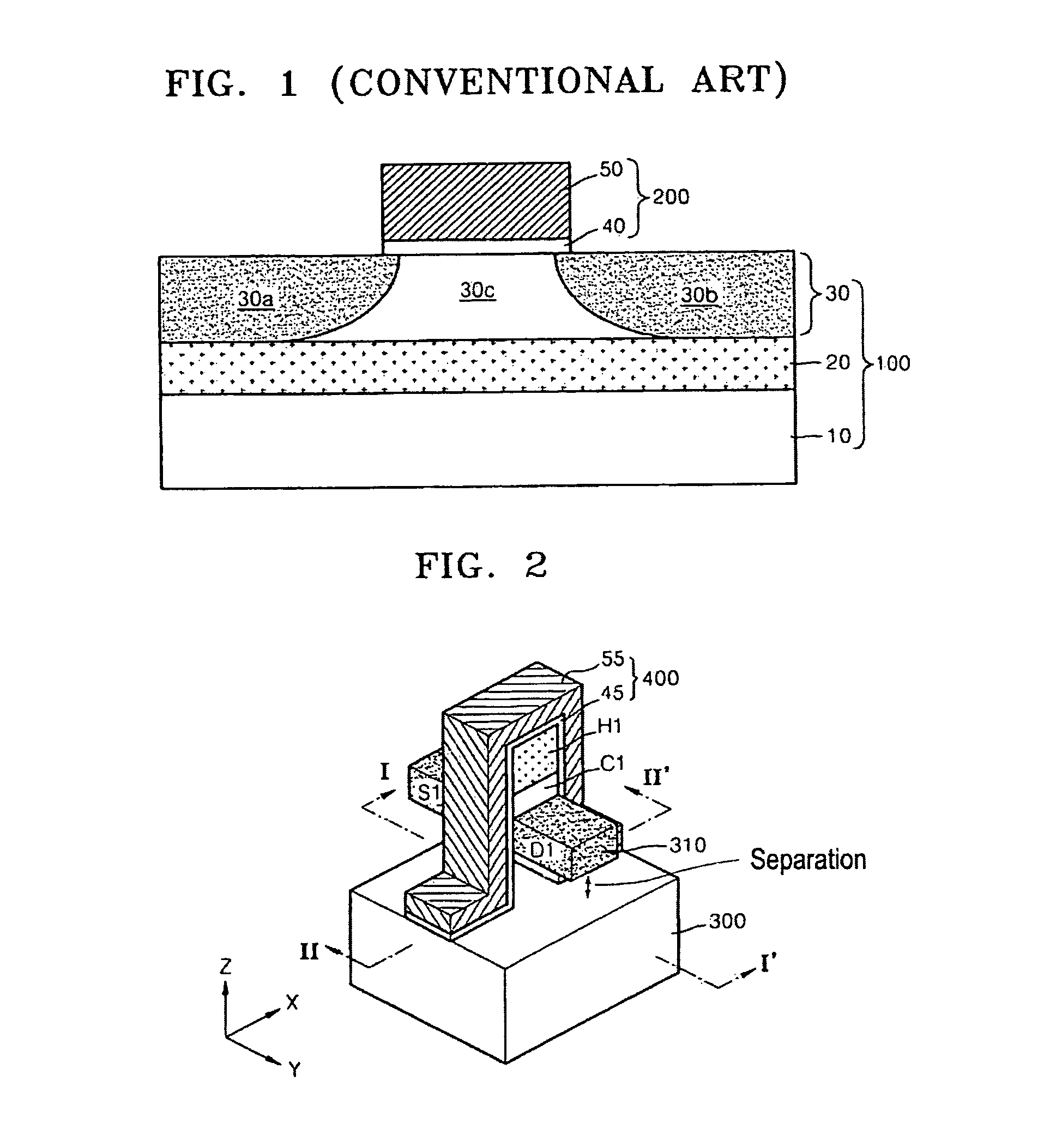
However, the data retention characteristics of the floating channel body 30c in the conventional capacitorless DRAM may not be desirable.
In addition, since the conventional capacitorless DRAM is formed on the expensive SOI substrate 100, increased manufacturing costs may be incurred.
Example embodiments are directed to a capacitorless dynamic random access memory (DRAM) that may have improved data retention characteristics, and which may result in decreased manufacturing costs.

Method used


Image

  • Capacitorless DRAM and methods of manufacturing and operating the same
  • Capacitorless DRAM and methods of manufacturing and operating the same
  • Capacitorless DRAM and methods of manufacturing and operating the same

Examples


Embodiment Construction

[0048]Detailed example embodiments are disclosed herein. However, specific structural and functional details disclosed herein are merely representative for purposes of describing example embodiments. Example embodiments may, however, be embodied in many alternate forms and should not be construed as limited to only the embodiments set forth herein.

[0049]Accordingly, while example embodiments are capable of various modifications and alternative forms, embodiments thereof are shown by way of example in the drawings and will herein be described in detail. It should be understood, however, that there is no intent to limit example embodiments to the particular forms disclosed, but to the contrary, example embodiments are to cover all modifications, equivalents, and alternatives falling within the scope of example embodiments. Like numbers refer to like elements throughout the description of the figures.

[0050]It will be understood that, although the terms first, second, etc. may be used h...


PUM


Abstract

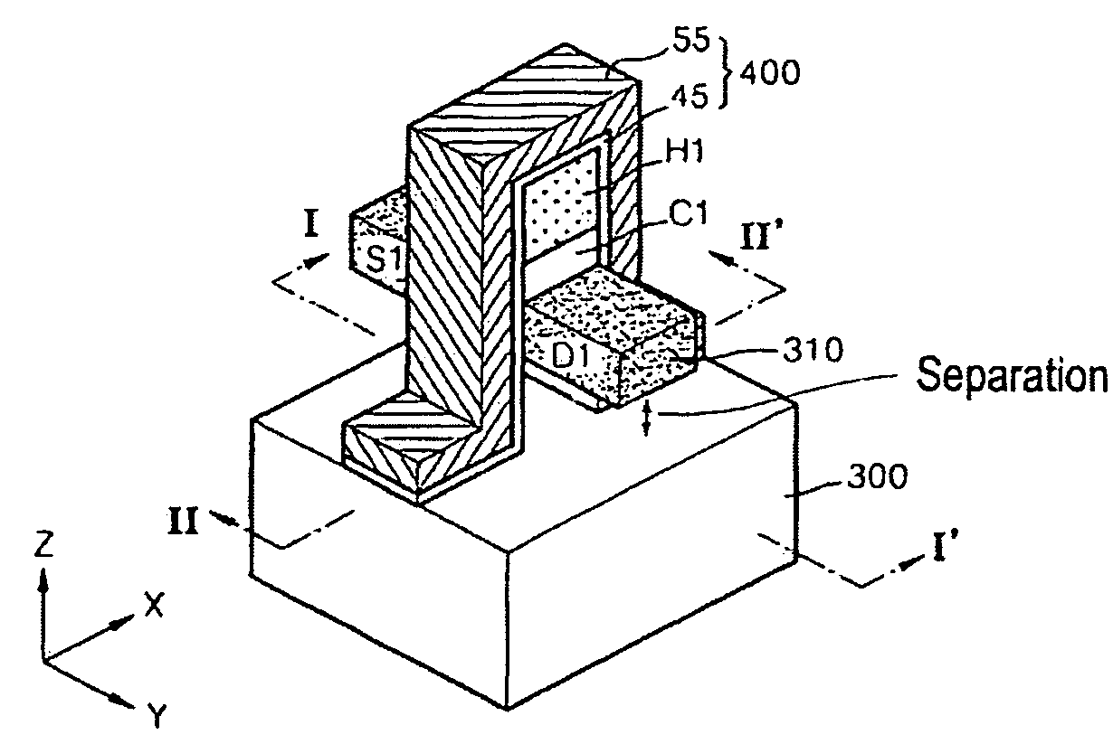
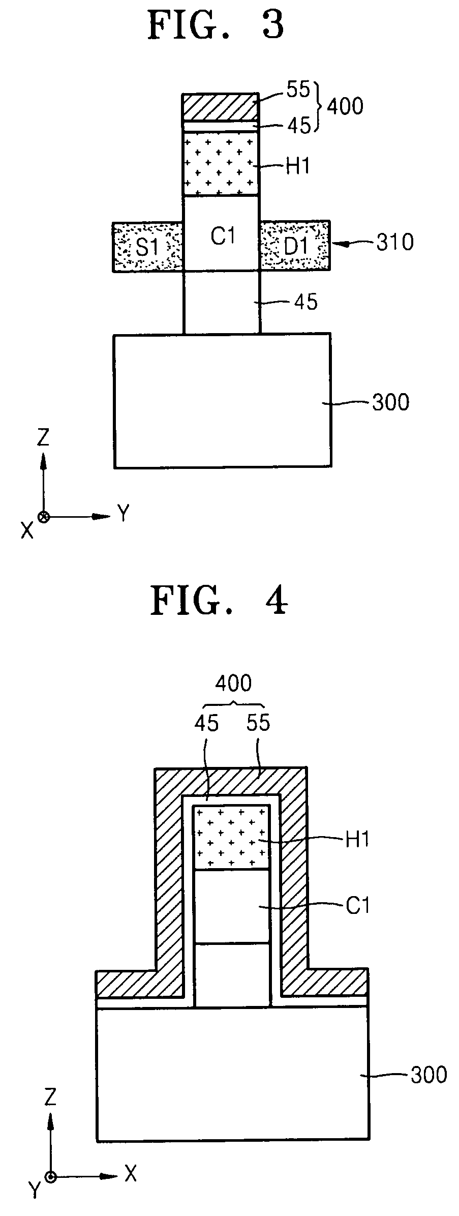
Example embodiments provide a capacitorless dynamic random access memory (DRAM), and methods of manufacturing and operating the same. The capacitorless DRAM according to example embodiments may include a semiconductor layer separated from a top surface of a substrate and that contains a source region, a drain region, and a channel region, a charge reserving layer formed on the channel region, and a gate formed on the substrate to contact the channel region and the charge reserving layer.

Description

FOREIGN PRIORITY STATEMENT[0001]This application claims priority under 35 U.S.C. §119 to Korean Patent Application No. 10-2007-0092149, filed on Sep. 11, 2007, in the Korean Intellectual Property Office, the entire contents of which are incorporated herein by reference.BACKGROUND[0002]1. Field[0003]Example embodiments are directed a semiconductor device and methods of manufacturing and operating the same, and more particularly, to a capacitorless dynamic random access memory (DRAM) and methods of manufacturing and operating the same.[0004]2. Description of Related Art[0005]A memory cell of a conventional dynamic random access memory (DRAM), may have a 1T / 1C structure including one transistor and one capacitor. It may be difficult to reduce a cell area of the conventional DRAM including both the transistor and the capacitor.[0006]In order to scale down conventional DRAMs, a DRAM that may store data with a transistor and without a capacitor, that is, a capacitorless 1T DRAM, has been ...

Claims


Application Information

Patent Timeline
Patent Type & Authority Patents(United States)
IPC IPC(8): H01L27/108H10B12/00
CPCH01L27/108H01L29/7841H01L27/10802H10B12/20H10B12/00
Inventor KIM, SUK-PILJIN, YOUNG-GUPARK, YOON-DONG
Owner SAMSUNG ELECTRONICS CO LTD
Learn More