Superconducting integrated circuit technology using iron-arsenic compounds

a technology of integrated circuits and iron-arsenic compounds, which is applied in the direction of superconducting magnets/coils, superconductor devices, magnetic bodies, etc., can solve the problems of insufficient technological usefulness of polycrystalline materials

Active Publication Date: 2011-11-08
HYPRES
View PDF5 Cites 19 Cited by
  • Summary
  • Abstract
  • Description
  • Claims
  • Application Information

AI Technical Summary

Benefits of technology

[0016]In addition to depositing thin films, microcircuits are patterned, preferably using photolithography. The patterns may be transferred to the films using one or more etch processes, such as argon and reactive-ion beam and plasma etches.
[0017]ICs based on high temperature superconducting Fe compound films, fabricated according to the provisions of this application, may comprise ultrafast RSFQ logic circuits operating at temperatures of 50 K or above.

Problems solved by technology

This is in sharp contrast to YBCO and the cuprates, where polycrystalline materials are not technologically useful for electronic applications.

Method used


Image

  • Superconducting integrated circuit technology using iron-arsenic compounds
  • Superconducting integrated circuit technology using iron-arsenic compounds
  • Superconducting integrated circuit technology using iron-arsenic compounds

Examples


Embodiment Construction

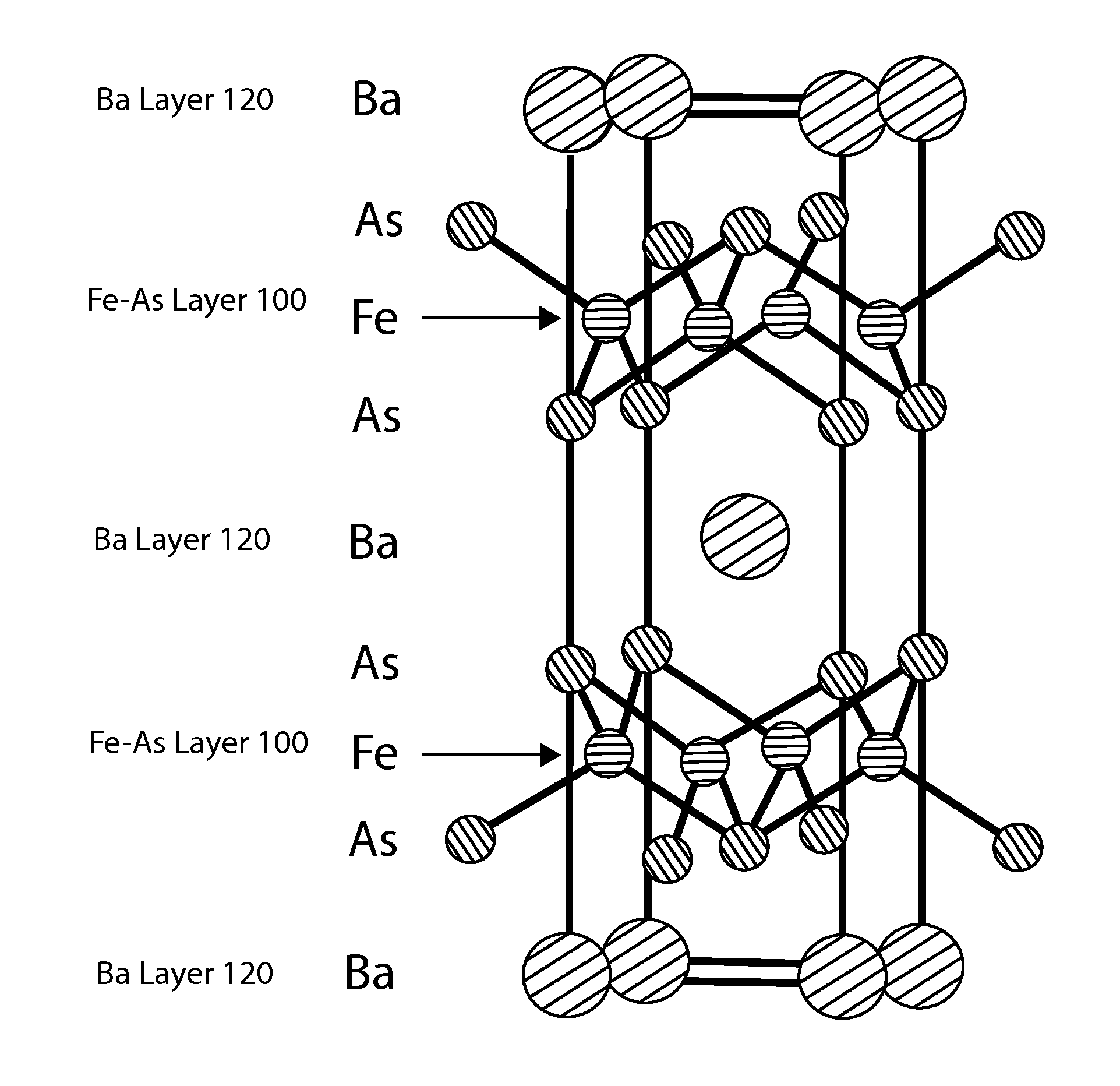
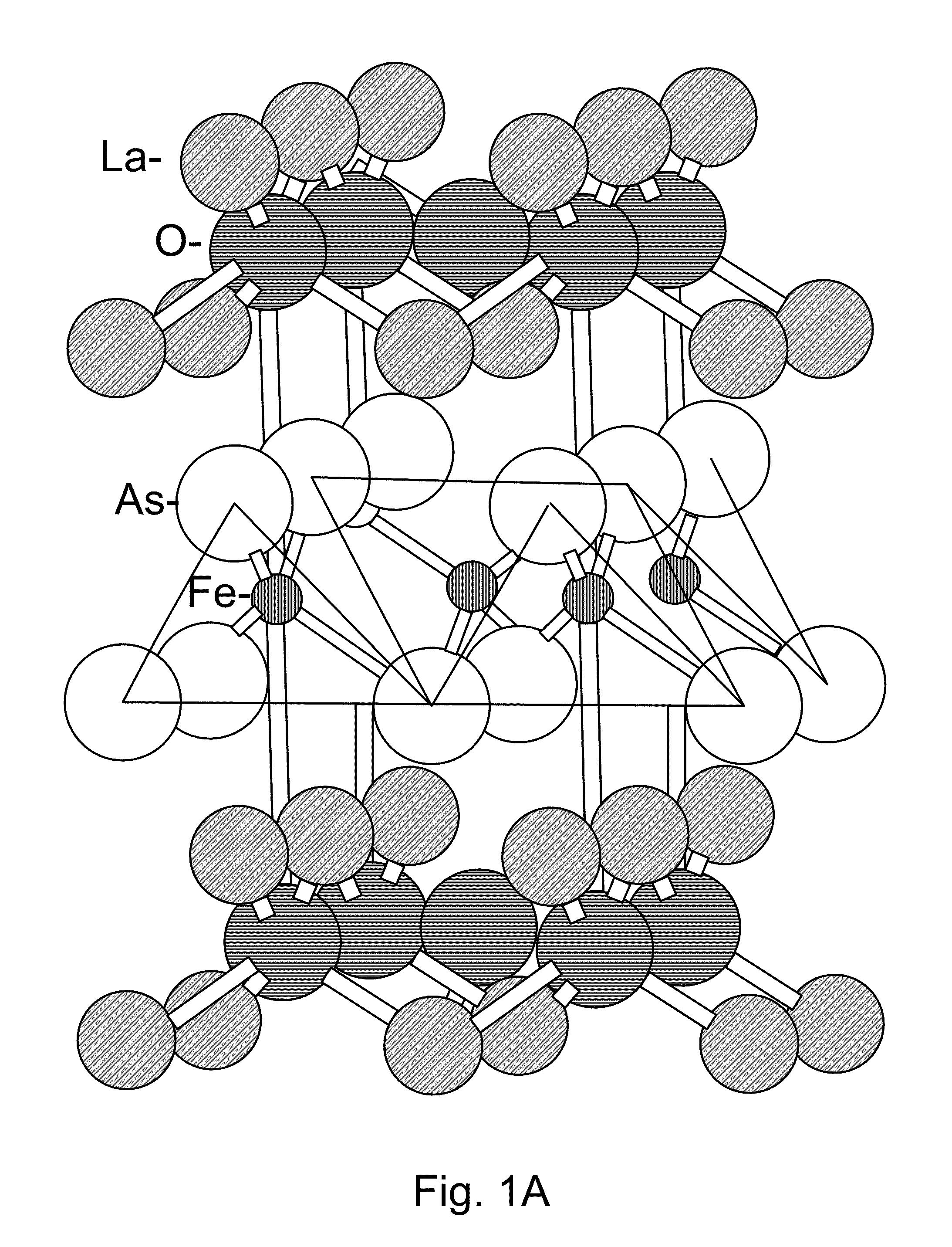
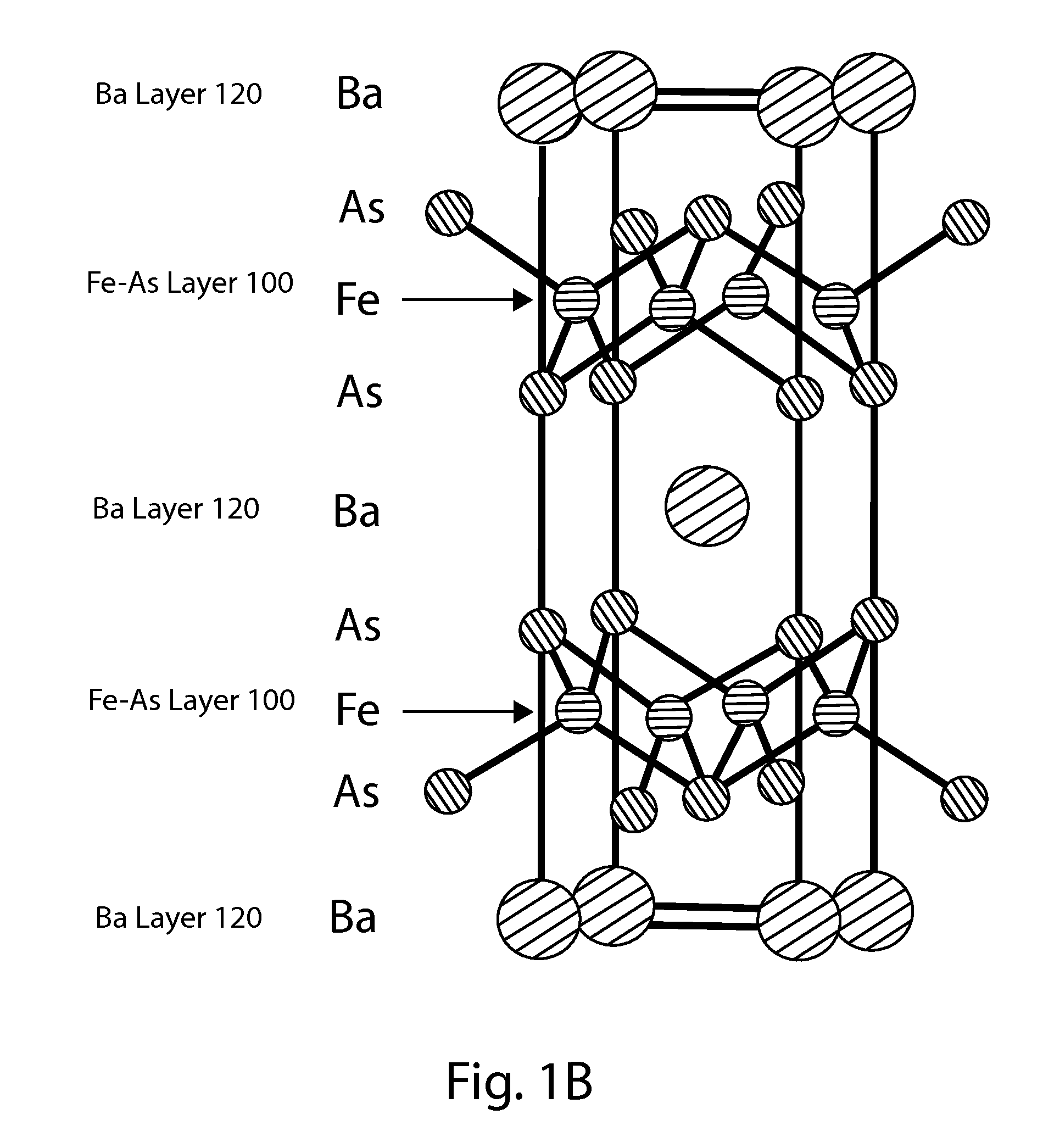
[0023]The crystal structure of LaFeAsO in FIG. 1A represents a family of closely related materials, some of which are superconductors at various temperatures. The crystal structure is tetragonal, with lattice constants a=b=0.4 nm and c=0.87 nm, with some variation in lattice parameters for elemental substitutions. The key functional part of this material is the planar network of Fe atoms in the a-b plane, surrounded by As atoms (the Fe—As layer 100 in FIG. 1A). The Fe atoms provide the conduction bands, and also the spin magnetic moments which may order magnetically. The La—O layers 110 are largely inert, but affect the FeAs layers in two major ways: they may “dope” the FeAs with electrons or holes, and they may structurally strain the FeAs layers. The Fe site may be substituted with other transition metal atoms such as Cr, Mn, Co, and Ni (adjacent in the periodic table). The As site may be substituted with P, just above it in the periodic table, or possibly Sb, just below it. Alter...


PUM

PropertyMeasurementUnit
critical temperatureaaaaaaaaaa
temperatureaaaaaaaaaa
thickaaaaaaaaaa

Abstract

A new family of superconducting materials with critical temperature up to 55 K have recently been discovered, comprising a crystal structure with atomic layers of iron and arsenic alternating with atomic layers of rare-earth oxide or alkaline earth. The present invention identifies structures for integrated circuit elements (including Josephson junctions) in these and related materials. These superconducting circuit elements will operate at a higher temperature than low-temperature superconductors such as niobium, and may be easier to manufacture than prior-art high-temperature superconductors based on copper-oxides.

Description

BACKGROUND OF THE INVENTION[0001]Thin-film devices based on superconducting materials have demonstrated superior performance for many applications. However, they will function properly only at deep cryogenic temperatures, below the critical temperature Tc of the given superconducting material. Conventional low-temperature superconductors (LTS) have been known for almost 100 years, and thin-film circuits based on the metallic element niobium (Nb) can be built around active devices known as Josephson junctions (JJ). These junctions form the basis for active superconducting electronic elements, both analog and digital. More specifically, large numbers of JJs can be integrated together using an ultra-fast circuit low-power technology known as RSFQ (rapid-single-flux-quantum) logic, which has provided digital integrated circuits (ICs) that are clocked at 100 GHz or more. However, these Nb-based circuits require cooling to below Tc=9 K to function. This is technologically feasible using c...

Claims


Application Information

Patent Timeline
Patent Type & Authority Patents(United States)
IPC IPC(8): H01L39/22
CPCH01L39/125H01L39/225H01L39/2496Y10S428/93Y10S505/817Y10S505/702H10N60/855H10N60/124H10N60/0941
Inventor KADIN, ALAN M.
Owner HYPRES
Why Eureka
Try Eureka