Method and program for designing semiconductor integrated circuit using peripheral parameter

a technology of integrated circuits and peripheral parameters, applied in the direction of program control, cad circuit design, instruments, etc., can solve the problems of not being able to module the spice model parameter of pmos transistor pb>1, not being able to consider the peripheral pattern dependence in spice simulation, and unable to achieve the effect of preventing the increase of design/verification ta

Inactive Publication Date: 2011-11-29
RENESAS ELECTRONICS CORP
View PDF19 Cites 1 Cited by
  • Summary
  • Abstract
  • Description
  • Claims
  • Application Information

AI Technical Summary

Benefits of technology

[0032]Therefore, the peripheral pattern dependence of the transistor characteristics is fully considered. The peripheral pattern dependence is fully considered in calculating the delay value of the target cell. Thus, the accuracy of the delay verification is improved. Consequently, yield and reliability of the semiconductor integrated circuit to be manufactured are also improved.
[0033]Moreover, since the above-mentioned delay function is generated at the characterization stage, it is not necessary to repeat the modulation of the SPICE netlist and the SPICE simulation at the circuit design / verification stage. By using the chip-level layout data and the delay function, it is possible to immediately calculate the cell delay value with considering the peripheral pattern dependence. Therefore, increase in the design / verification TAT can be prevented.
[0034]Furthermore, the margin such as shown in FIG. 4 is not added to the delay value of each cell which is calculated based on the chip-level layout data and the delay function. Although a center value of the calculated cell delay value may vary from the normal one, the variability range is the same as the normal one. As a result, the number of repetition times of the layout design and delay verification is prevented from being increased. Therefore, the increase in the design / verification TAT can be prevented. Moreover, it is not necessary to increase driving capability of transistors and / or to additionally insert redundant cells. Therefore, the increase in the chip area and power consumption can be prevented.
[0037]According to the present invention, it is possible to prevent the increase in the design / verification TAT for the semiconductor integrated circuit, while considering the peripheral pattern dependence of the transistor characteristics sufficiently.

Problems solved by technology

Due to the OPE, a resist pattern may not be formed as intended, which causes deviations of interconnection width and gate size from the design values.
Therefore, it is not possible to module the SPICE model parameter of the PMOS transistor P1 prior to the SPICE simulation.
However, with regard to the outermost transistor placed near the cell boundary, it is not possible to consider the peripheral pattern dependence in the SPICE simulation since the peripheral layout pattern is unknown.
Consequently, it cannot be said that the accuracy of the delay verification (STA) is sufficient.
This contributes to reduction of yield and reliability of the semiconductor integrated circuit to be manufactured.
Furthermore, the first method is disadvantageous in that the corner condition of the cell delay value becomes stricter as compared with that in the method shown in FIG. 2. FIG. 4 schematically shows the corner condition (corner delay value) provided by the cell delay library.
In other words, it is necessary to repeat the layout design and delay verification until the design circuit operates in the corner condition.
This leads to increase in a chip area and power consumption.

Method used


Image

  • Method and program for designing semiconductor integrated circuit using peripheral parameter
  • Method and program for designing semiconductor integrated circuit using peripheral parameter
  • Method and program for designing semiconductor integrated circuit using peripheral parameter

Examples


Embodiment Construction

[0052]The invention will be now described herein with reference to illustrative embodiments. Those skilled in the art will recognize that many alternative embodiments can be accomplished using the teachings of the present invention and that the invention is not limited to the embodiments illustrated for explanatory purposed.

[0053]1. Outline

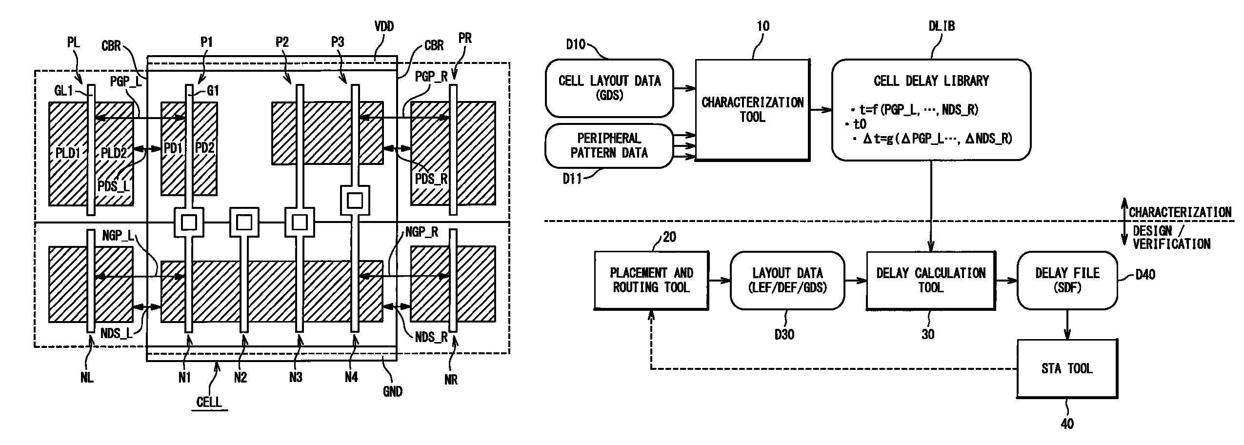
[0054]According to the present embodiment, the peripheral pattern dependence of the transistor characteristics is considered. In particular, a layout pattern around a cell is considered at the time of characterization of the cell. The layout pattern around a cell is referred to as “peripheral pattern”. The peripheral pattern affects characteristics of a transistor placed at the outermost in the cell.

[0055]FIG. 5 is a plan view for explaining the peripheral pattern of a certain cell. As an example, let us consider a primitive cell such as a NAND gate, an inverter or the like. The cell shown in FIG. 5 has PMOS transistors P1 to P3 and NMOS transisto...


PUM


Abstract

A method of designing a semiconductor integrated circuit includes: performing a circuit simulation of a cell with changing a parameter that specifies a layout pattern around the cell; and generating a delay function expressing a delay value of the cell as a function of the parameter, based on a result of the circuit simulation. The method further includes: generating a layout data indicating a layout of the semiconductor integrated circuit, based on a cell-based design technique. The method further includes: referring to the generated layout data to extract the parameter associated with a target cell included in the semiconductor integrated circuit; and calculating a delay value of the target cell by using the extracted parameter and the delay function.

Description

INCORPORATION BY REFERENCE[0001]This application is based upon and claims the benefit of priority from Japanese patent application No. 2007-185924, filed on Jul. 17, 2007, the disclosure of which is incorporated herein in its entirely by reference.BACKGROUND OF THE INVENTION[0002]1. Field of the Invention[0003]The present invention relates to a design technique for a semiconductor integrated circuit. In particular, the present invention relates to a design technique in which layout around an element is considered.[0004]2. Description of Related Art[0005]Characteristics of a transistor depend on “device parameters” such as gate length L, gate width W, mobility μ, threshold voltage Vt and the like. When the transistor is actually manufactured, those device parameters are likely to vary from design values. The variations of the device parameters from the design values lead to variations of the transistor characteristics from expected values. It is therefore important to sufficiently co...

Claims


Application Information

Patent Timeline
Patent Type & Authority Patents(United States)
IPC IPC(8): G06F17/50
CPCG06F17/5036G06F17/5068G06F30/367G06F30/39
Inventor YAMADA, KENTA
Owner RENESAS ELECTRONICS CORP
Why Eureka
Try Eureka