Stacked electronic component package having film-on-wire spacer

a technology of electronic components and film-on-wires, which is applied in the direction of electrical apparatus contruction details, fluid pressure measurement, instruments, etc., can solve the problems of reducing so as to reduce the stress on the upper electronic component and the chance of cracking the upper electronic componen

Active Publication Date: 2011-12-06
AMKOR TECH SINGAPORE HLDG PTE LTD
View PDF245 Cites 10 Cited by
  • Summary
  • Abstract
  • Description
  • Claims
  • Application Information

AI Technical Summary

Benefits of technology

[0010]In accordance with one embodiment, a film-on-wire spacer covers an entire upper surface of a lower electronic component and the lower bond wires. Accordingly, an upper electronic component is supported above bond pads and lower bond wires of the lower electronic component. This decreases the stress on the upper electronic component, e.g., during wirebonding, and thus decreases the chance of cracking the upper electronic component. Further, the lower bond wires are enclosed in and protected by the film-on-wire spacer. Further, the film-on-wire spacer is thin resulting in a minimum height of the stacked electronic component package.

Problems solved by technology

This decreases the stress on the upper electronic component, e.g., during wirebonding, and thus decreases the chance of cracking the upper electronic component.
Further, the film-on-wire spacer is thin resulting in a minimum height of the stacked electronic component package.

Method used


Image

  • Stacked electronic component package having film-on-wire spacer
  • Stacked electronic component package having film-on-wire spacer
  • Stacked electronic component package having film-on-wire spacer

Examples


Embodiment Construction

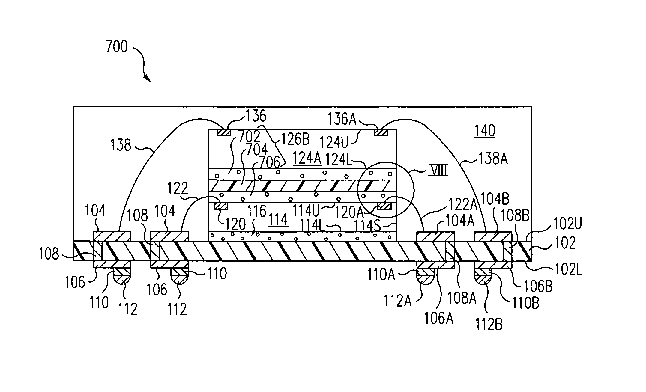
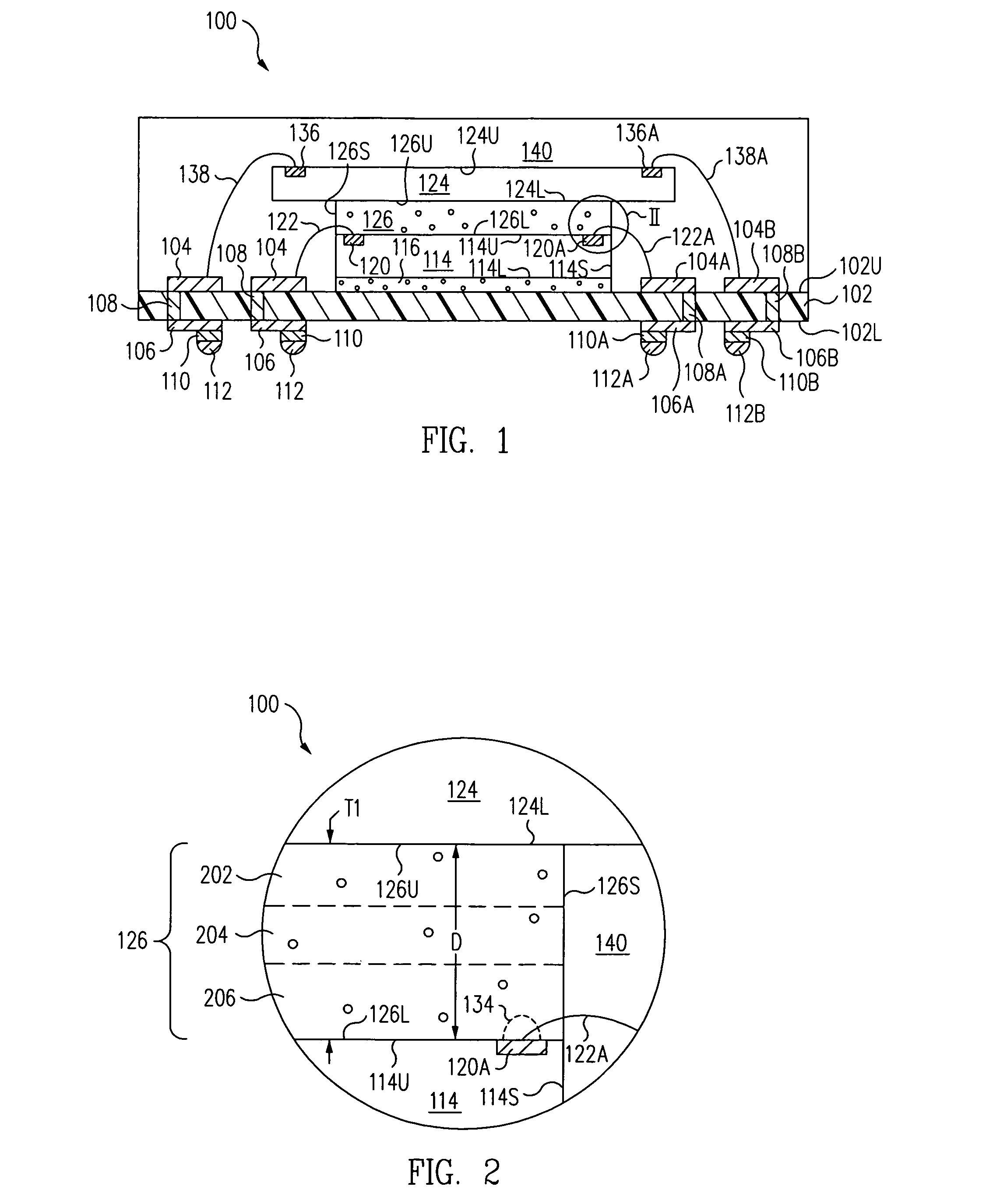
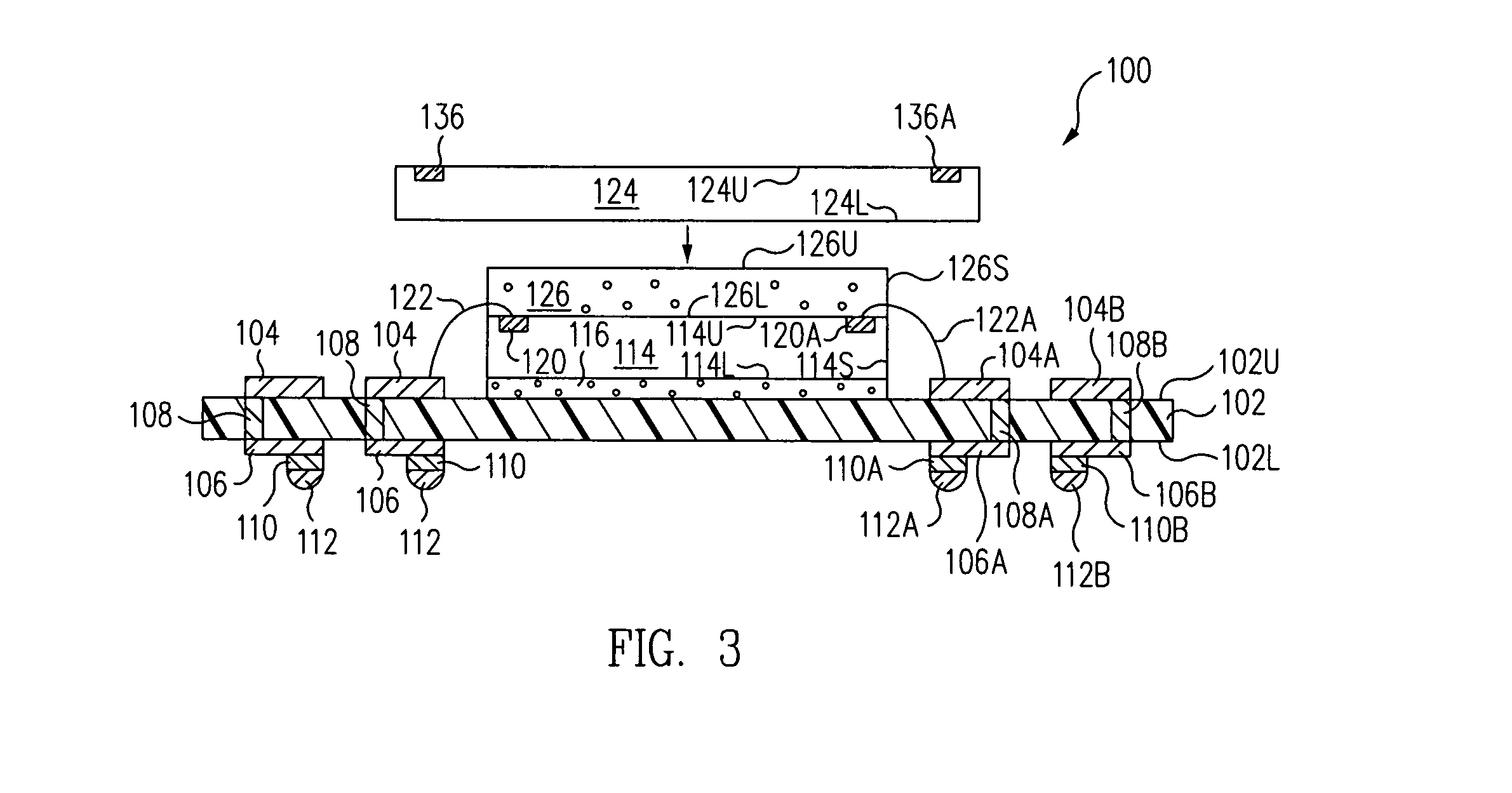
[0031]In accordance with one embodiment, referring to FIGS. 1 and 2 together, a film-on-wire spacer 126 covers an entire upper surface 114U of a lower electronic component 114. Accordingly, an upper electronic component 124 is supported above bond pads 120 and lower bond wires 122 of lower electronic component 114. This decreases the stress on upper electronic component 124, e.g., during wirebonding, and thus decreases the chance of cracking upper electronic component 124. Further, lower bond wires 122 are enclosed in and protected by film-on-wire spacer 126. Further, film-on-wire spacer 126 is thin resulting in a minimum height of stacked electronic component package 100.

[0032]More particularly, FIG. 1 is a cross-sectional view of a stacked electronic component package 100 in accordance with one embodiment of the present invention. Stacked electronic component package 100 includes a substrate 102, e.g., formed of metal, with ceramic, pre-molded plastic or laminate materials, althou...


PUM


Abstract

A film-on-wire spacer covers an entire upper surface of a lower electronic component. Accordingly, an upper electronic component is supported above bond pads and lower bond wires of the lower electronic component. This decreases the stress on the upper electronic component, e.g., during wirebonding, and thus decreases the chance of cracking the upper electronic component. Further, the lower bond wires are enclosed in and protected by the film-on-wire spacer. Further, the film-on-wire spacer is thin resulting in a minimum height of the stacked electronic component package.

Description

RELATED APPLICATIONS[0001]This application is a divisional of St. Amand et al., U.S. patent application Ser. No. 11 / 356,921, filed on Feb. 17, 2006, entitled “STACKED ELECTRONIC COMPONENT PACKAGE HAVING FILM-ON-WIRE SPACER”, now U.S. Pat. No. 7,675,180, issued Mar. 9, 2010, which is herein incorporated by reference in its entirety.BACKGROUND OF THE INVENTION[0002]1. Field of the Invention[0003]The present invention relates generally to the packaging of electronic components. More particularly, the present invention relates to a stacked electronic component package and method for fabricating the same.[0004]2. Description of the Related Art[0005]To reduce the size of electronic component packages, electronic components such as semiconductor dies were stacked one upon another within a stacked electronic component package. To space the upper electronic component above the lower bond wires connected to the bond pads of the lower electronic component, a spacer was used.[0006]The spacer wa...

Claims


Application Information

Patent Timeline
Patent Type & Authority Patents(United States)
IPC IPC(8): H01L23/52H01L23/48H01L29/40
CPCB81C1/0023G01L19/0084G01L19/141H01L23/49582H01L24/29H01L24/32H01L24/33H01L24/48H01L24/73H01L24/83H01L25/0657B81B2201/0264B81B2207/07B81C2201/019H01L23/49548H01L23/49816H01L23/49861H01L24/45H01L27/14618H01L2224/27013H01L2224/274H01L2224/32014H01L2224/32145H01L2224/32225H01L2224/32245H01L2224/45144H01L2224/48091H01L2224/48227H01L2224/48247H01L2224/48465H01L2224/48599H01L2224/4899H01L2224/49175H01L2224/73265H01L2224/83051H01L2224/83191H01L2224/83192H01L2224/83856H01L2224/8592H01L2224/92247H01L2225/0651H01L2225/06562H01L2225/06575H01L2924/01005H01L2924/01013H01L2924/01014H01L2924/01027H01L2924/01029H01L2924/01078H01L2924/01079H01L2924/01082H01L2924/014H01L2924/14H01L2924/15311H01L2924/19041H01L2924/19042H01L2924/19043H01L24/49H01L2224/29H01L2224/2919H01L2224/29298H01L2924/01033H01L2924/0665H01L2224/29101H01L2224/2929H01L2924/00013H01L2924/1815H01L2224/83139H01L2924/15747H01L2924/1461H01L2924/00014H01L2924/00H01L2924/00012H01L2924/3512H01L2224/29099H01L2224/29199H01L2224/29299H01L2924/181H01L2224/2612H01L2224/85399H01L2224/05599
Inventor ST. AMAND, ROGER D.HAN, CHANGSUKKIM, YOUNSANGPARK, KYUNGROKPERELMAN, VLADIMIR
Owner AMKOR TECH SINGAPORE HLDG PTE LTD
Why Eureka
Try Eureka