Semiconductor integrated circuit including column redundancy fuse block

a technology of integrated circuits and fuse blocks, which is applied in the field of semiconductor integrated circuits, can solve the problems of reducing the product yield of semiconductor devices, increasing the density of devices, and reducing the layout of interconnections and circuits, and achieves the effect of improving alignment efficiency

Active Publication Date: 2011-12-13
SK HYNIX INC
View PDF17 Cites 14 Cited by
  • Summary
  • Abstract
  • Description
  • Claims
  • Application Information

AI Technical Summary

Benefits of technology

[0013]A semiconductor integrated circuit capable of improving the alignment efficiency is described herein.

Problems solved by technology

Accordingly, the defect density of the devices also increases, thereby lowering product yield of semiconductor devices.
Thus, there are limitations in the layout of the interconnections and the circuits.
This makes it difficult to ensure the effective net die of the semiconductor chip.

Method used


Image

  • Semiconductor integrated circuit including column redundancy fuse block
  • Semiconductor integrated circuit including column redundancy fuse block
  • Semiconductor integrated circuit including column redundancy fuse block

Examples


Embodiment Construction

.”

BRIEF DESCRIPTION OF THE DRAWINGS

[0018]Features, aspects, and embodiments are described in conjunction with the attached drawings, in which:

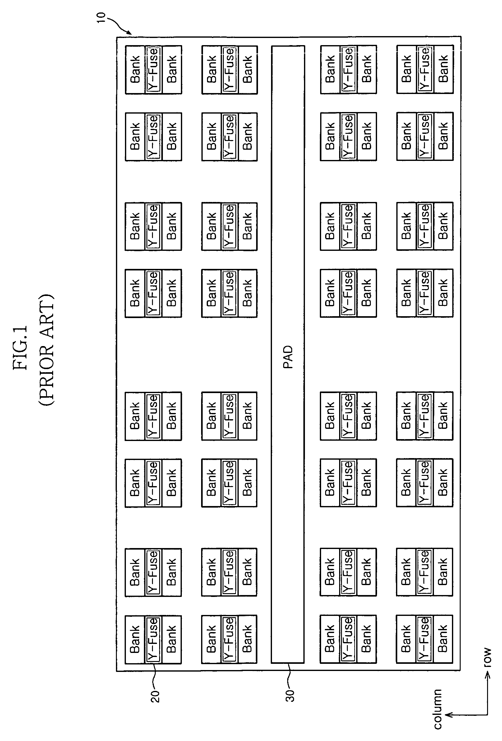
[0019]FIG. 1 is a plan view of a conventional semiconductor chip;

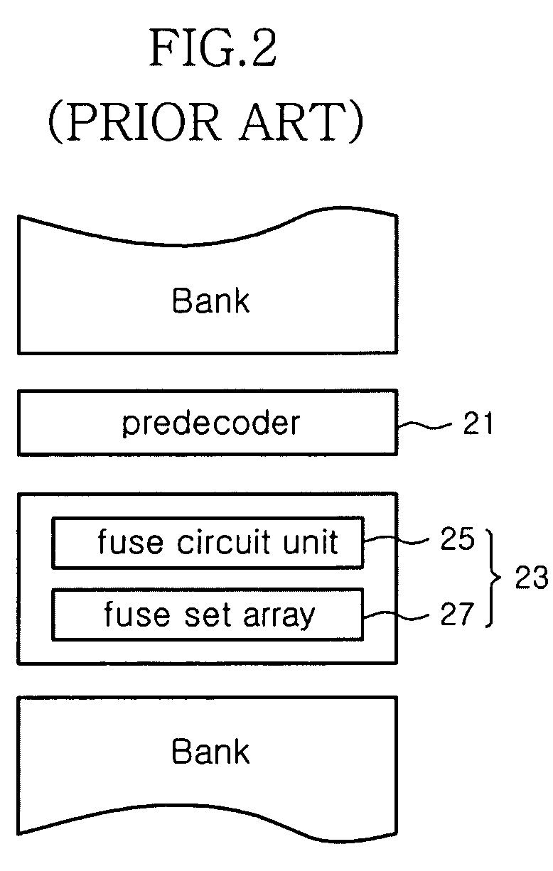
[0020]FIG. 2 is a block diagram of a conventional redundancy circuit unit of a semiconductor chip;

[0021]FIG. 3 is a plan view of an exemplary semiconductor chip according to one embodiment;

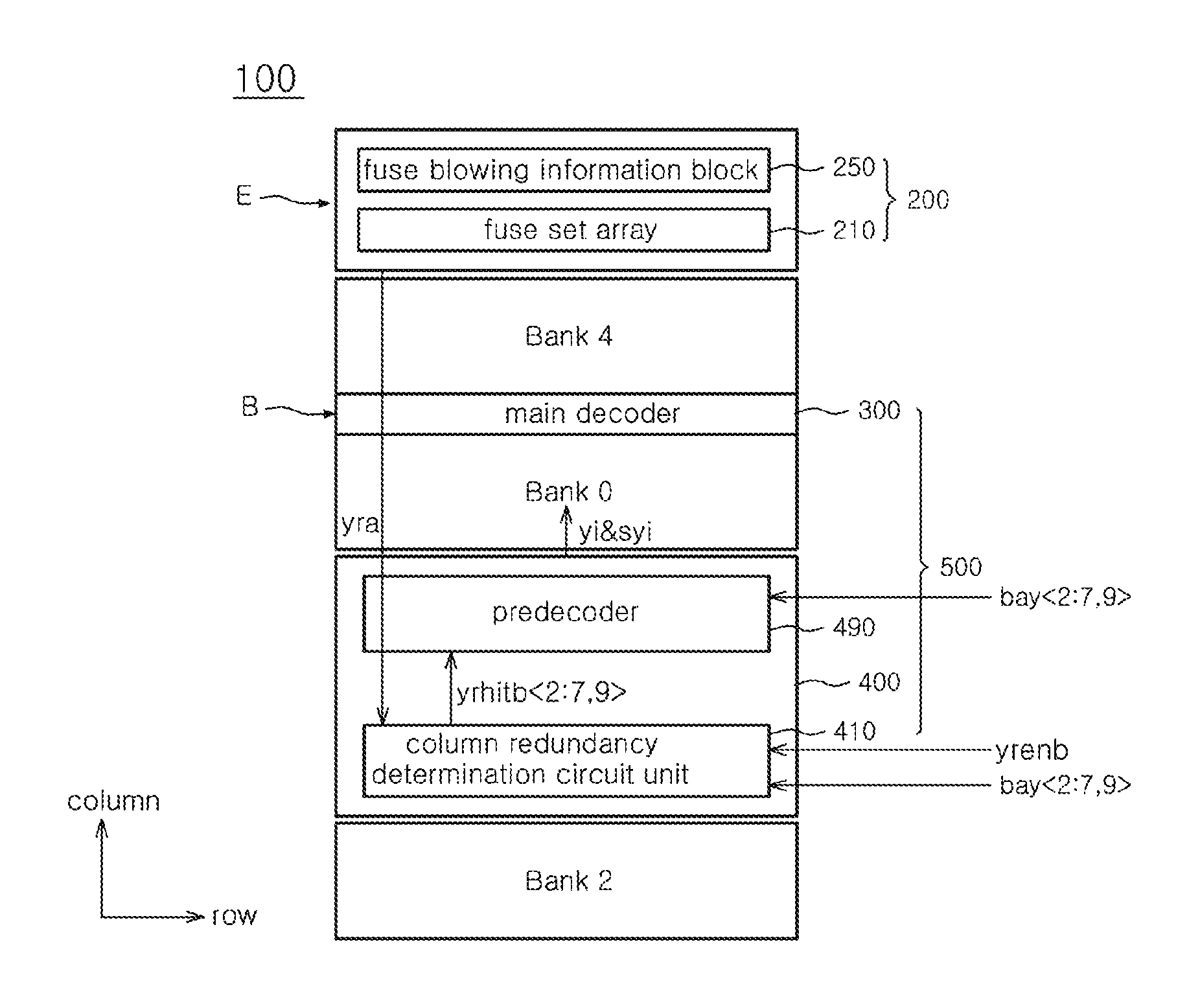
[0022]FIG. 4 is an enlarged block view of an ‘X’ portion of FIG. 3 according to one embodiment;

[0023]FIG. 5A is a plan view of an exemplary relation between a unit fuse set and a mat according to one embodiment;

[0024]FIG. 5B is a plan view of an exemplary fuse set according to one embodiment;

[0025]FIG. 5c is a plan view of another exemplary fuse set according to another embodiment;

[0026]FIG. 6 is a block view of an exemplary fuse determination circuit block according to one embodiment;

[0027]FIG. 7 is a schematic circuit of an exemplary fuse enable circuit unit according to one embodiment;

[0028]...


PUM


Abstract

A semiconductor integrated circuit includes a semiconductor chip having an edge area and a bank area located an inner portion of the edge area, and a column redundancy fuse block disposed in the edge area.

Description

CROSS-REFERENCES TO RELATED APPLICATION[0001]The present application claims priority under 35 U.S.C. 119(a) to Korean application numbers 10-2008-0004850 and 10-2008-122599, filed on Jan. 16, 2008 and Dec. 4, 2008, respectively, in the Korean Intellectual Property Office, which are incorporated herein by reference in their entirety as if set forth in full.BACKGROUND[0002]1. Technical Field[0003]The embodiments described herein relate to a semiconductor integrated circuit, and more particularly, to a semiconductor integrated circuit including a column redundancy fuse block.[0004]2. Related Art[0005]As the scaled size of semiconductor integrated circuits are reduced, the number of devices integrated in a single semiconductor chip has increased. Accordingly, the defect density of the devices also increases, thereby lowering product yield of semiconductor devices. In extreme cases, a wafer used for manufacturing the semiconductor devices must be discarded.[0006]In order to reduce the de...

Claims


Application Information

Patent Timeline
Patent Type & Authority Patents(United States)
IPC IPC(8): G11C7/00G11C29/00
CPCG11C29/785G11C2229/763
Inventor SONG, KEUN-SOOPARK, NAK-KYU
Owner SK HYNIX INC
Why Eureka
Try Eureka