

Automatic aligner
A technology of automatic alignment and alignment holes, which is applied in the direction of exposure devices, instruments, electrical components, etc. in the photoplate making process, can solve the problems of unsatisfactory alignment errors, increase production costs, and time-consuming, so as to meet strict requirements and avoid Error, the effect of improving alignment efficiency
- Summary
- Abstract
- Description
- Claims
- Application Information
AI Technical Summary
Problems solved by technology
Method used
Image

Examples
Embodiment Construction
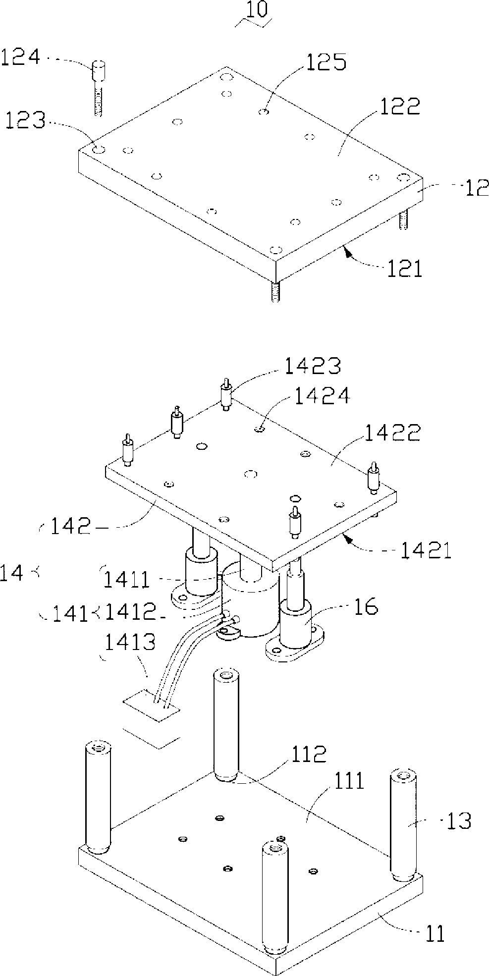
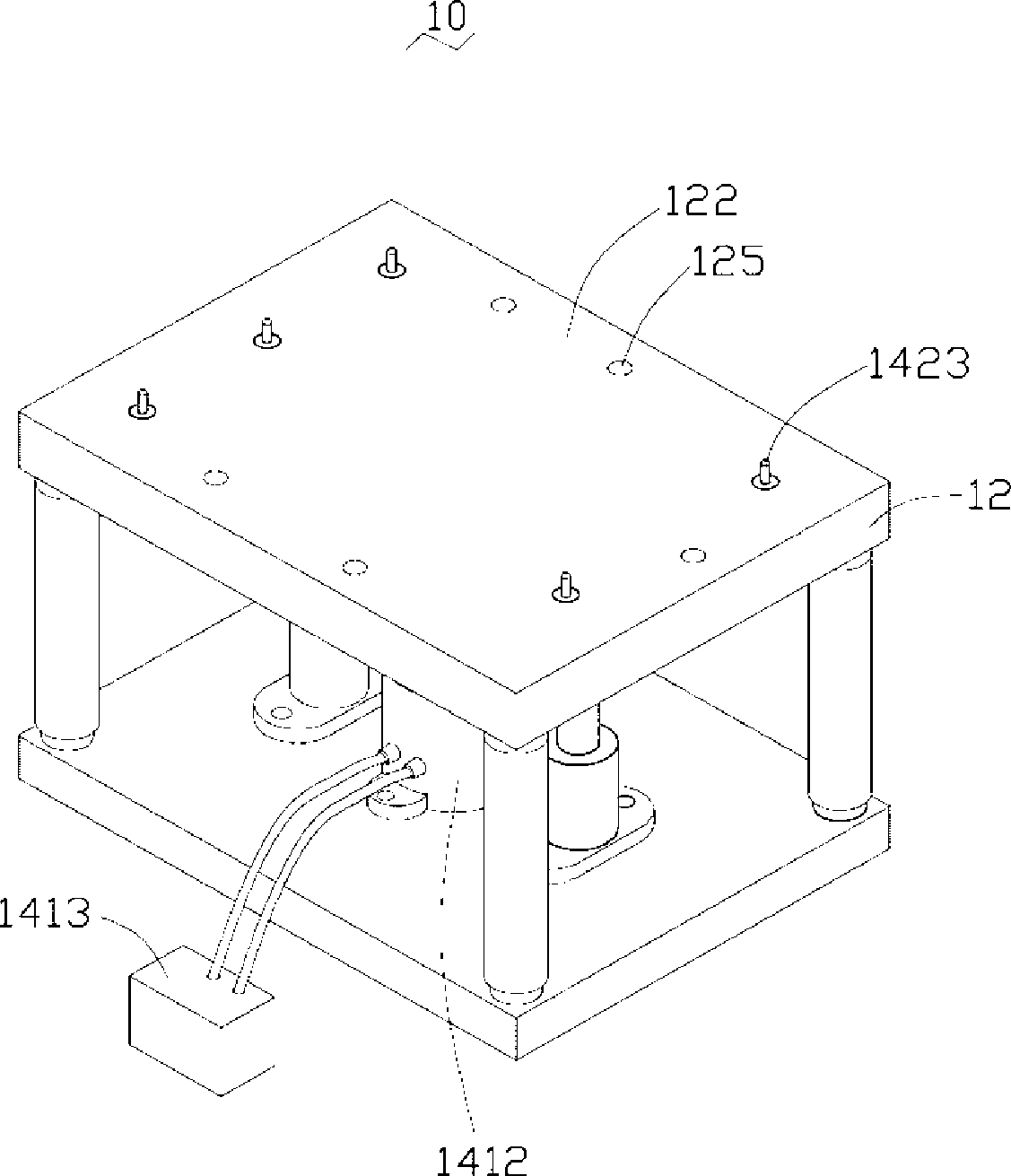
[0012] The automatic alignment device provided by the embodiment of the technical solution will be further described below in conjunction with the drawings and embodiments.
[0013] Please also refer to figure 1 and figure 2 , is the automatic alignment device 10 provided by the embodiment of the technical solution, which includes a base 11 , a carrying platform 12 , a support 13 and a lifting device 14 . The supporting member 13 and the lifting device 14 are located between the base 11 and the carrying platform 12 .
[0014] The base 11 has a base surface 111 . The base surface 111 is opposite to the carrying platform 12 and is used for setting the carrying platform 12 , the supporting member 13 and the lifting device 14 . In this embodiment, the abutment surface 111 of the abutment 11 defines a first fixing hole 112 for fixing the supporting member 13 . The first fixing holes 112 are located at the four corners of the abutment surface 111 for matching with the support m...
PUM
| Property | Measurement | Unit |
|---|---|---|
| diameter | aaaaa | aaaaa |
Abstract
Description
Claims
Application Information