Registered structure formation via the application of directed thermal energy to diblock copolymer films

a technology of copolymer film and registered structure, applied in the field of registered structure formation via the application of directed thermal energy to diblock copolymer film, can solve the problems of not being able to realize manufacturable process, unable to accommodate structures and features much below 100 nm level, and conventional optical lithographic processing methods cannot accommodate structure fabrication and features

Active Publication Date: 2011-12-27
MICRON TECH INC
View PDF193 Cites 99 Cited by
  • Summary
  • Abstract
  • Description
  • Claims
  • Application Information

AI Technical Summary

Problems solved by technology

Conventional optical lithographic processing methods are not able to accommodate fabrication of structures and features much below the 100 nm level.
Although registered and ordered arrays of cylinders have been produced within trenches, the fabrication of an ordered array of repeat structures outside of the confines of trenches and over large areas has not been realized in a manufacturable process.

Method used


Image

  • Registered structure formation via the application of directed thermal energy to diblock copolymer films
  • Registered structure formation via the application of directed thermal energy to diblock copolymer films
  • Registered structure formation via the application of directed thermal energy to diblock copolymer films

Examples


Embodiment Construction

The following description with reference to the drawings provides illustrative examples of devices and methods according to embodiments of the invention. Such description is for illustrative purposes only and not for purposes of limiting the same.

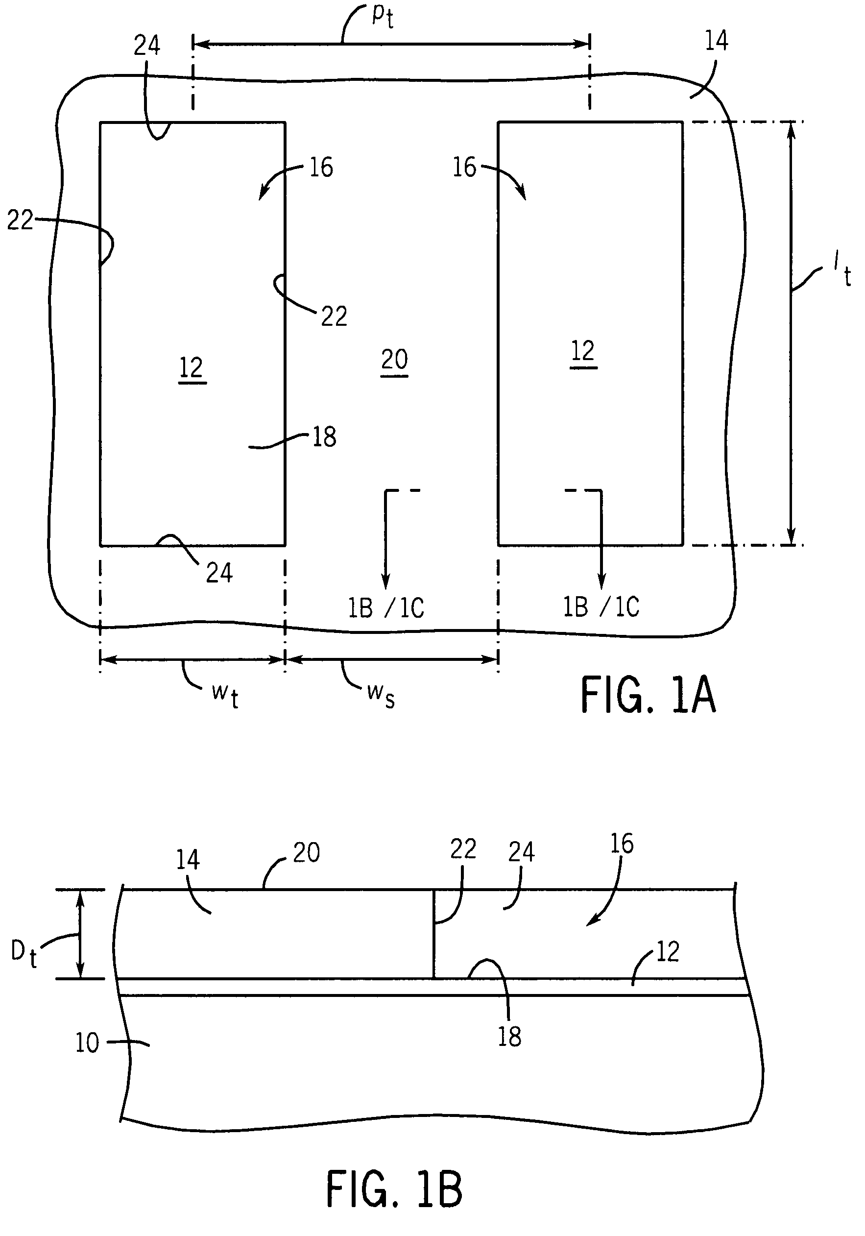
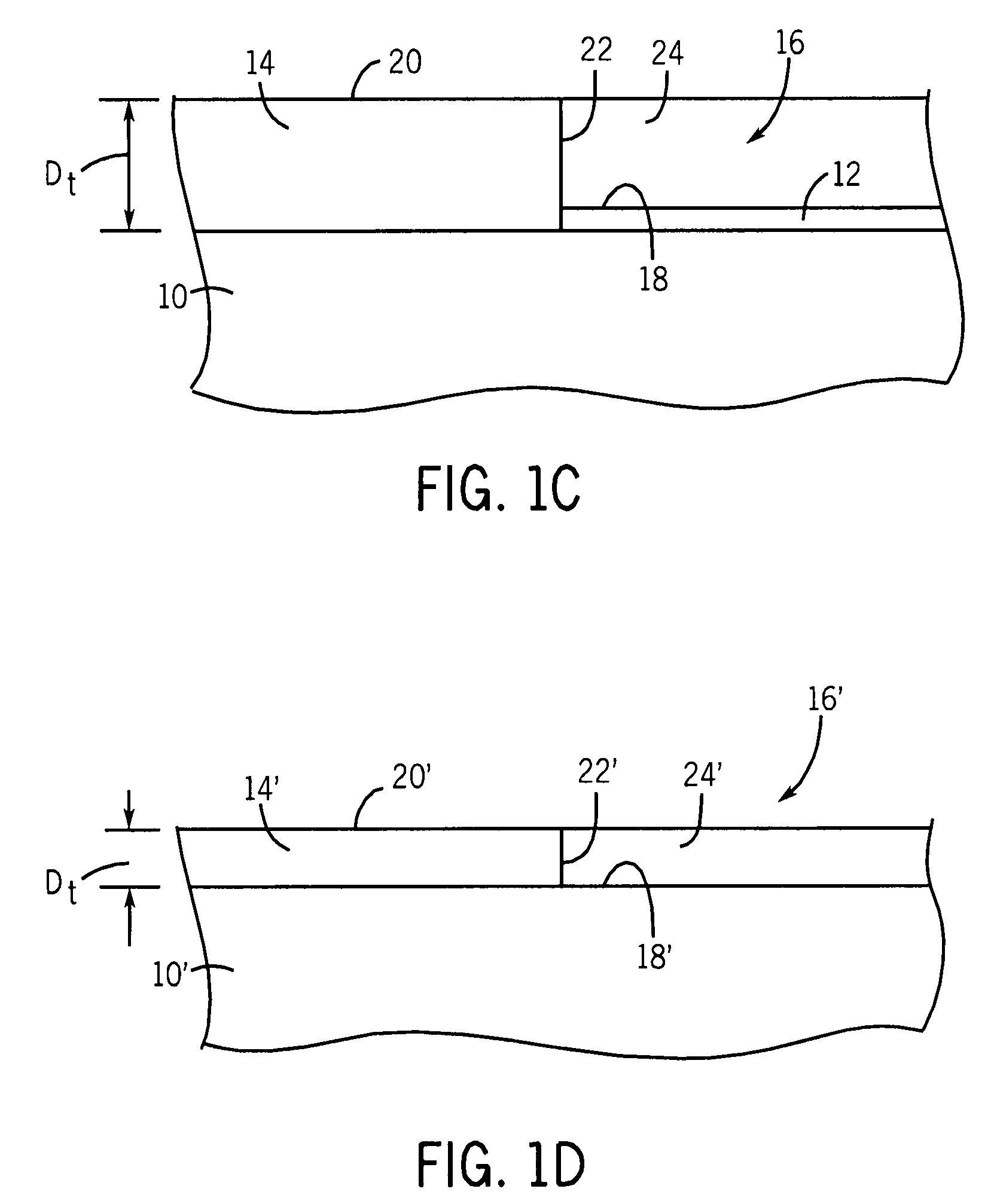
In the context of the current application, the term “semiconductor substrate” or “semiconductive substrate” or “semiconductive wafer fragment” or “wafer fragment” or “wafer” will be understood to mean any construction comprising semiconductor material, including but not limited to bulk semiconductive materials such as a semiconductor wafer (either alone or in assemblies comprising other materials thereon), and semiconductive material layers (either alone or in assemblies comprising other materials). The term “substrate” refers to any supporting structure including, but not limited to, the semiconductive substrates, wafer fragments or wafers described above.

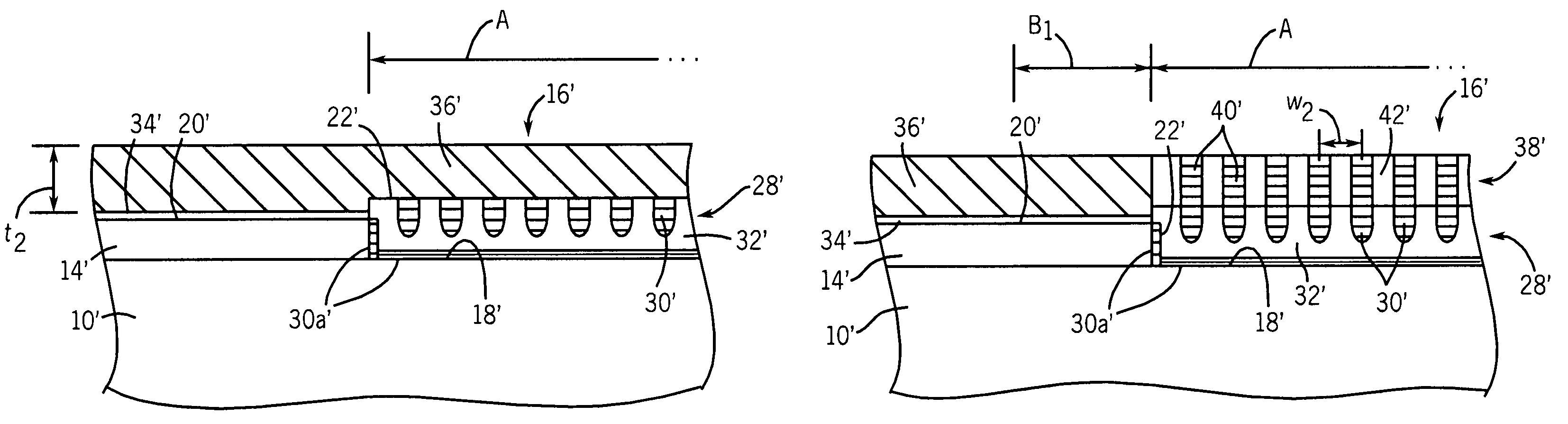
“Lo” is the inherent pitch (bulk period or repeat unit) of structures that self assem...


PUM

PropertyMeasurementUnit
thickaaaaaaaaaa
lengthaaaaaaaaaa
lengthaaaaaaaaaa

Abstract

Methods for fabricating sublithographic, nanoscale linear microchannel arrays over surfaces without defined features utilizing self-assembling block copolymers, and films and devices formed from these methods are provided. Embodiments of the methods use a multilayer induced ordering approach to align lamellar films to an underlying base film within trenches, and localized heating to anneal the lamellar-phase block copolymer film overlying the trenches and outwardly over the remaining surface.

Description

TECHNICAL FIELDEmbodiments of the invention relate to methods of fabricating nanoscale linear arrays of microstructures and microchannels by use of thin films of self-assembling block copolymers, and devices resulting from those methods.BACKGROUND OF THE INVENTIONAs the development of nanoscale mechanical, electrical, chemical and biological devices and systems increases, new processes and materials are needed to fabricate nanoscale devices and components. Conventional optical lithographic processing methods are not able to accommodate fabrication of structures and features much below the 100 nm level. The use of self assembling diblock copolymers presents another route to patterning at nanometer dimensions. Diblock copolymer films spontaneously assembly into periodic structures by microphase separation of the constituent polymer blocks after annealing, for example by thermal annealing above the glass transition temperature of the polymer or by solvent annealing, forming ordered dom...

Claims


Application Information

Patent Timeline
Patent Type & Authority Patents(United States)
IPC IPC(8): B44C1/22H01L21/302B82B3/00
CPCB82Y30/00B82Y10/00B81C1/00031C08L53/00B81B1/00B82Y40/00B81C1/00015Y10T428/24744Y10S438/947Y10S977/90Y10S977/895Y10S977/888B81C2201/0198B81C2201/0149G03F7/0002Y10T428/24612Y10T428/24479C08L2666/02
Inventor MILLWARD, DAN B.MARSH, EUGENE P.
Owner MICRON TECH INC
Why Eureka
Try Eureka