Electrical current distribution in light emitting devices

a technology of light emitting devices and current distribution, which is applied in the direction of electric devices, solid-state devices, basic electric elements, etc., can solve the problems of significant reduction in light output, and achieve the effect of minimizing its effect on light outpu

Inactive Publication Date: 2012-02-28
TINGGI TECH PTE
View PDF157 Cites 4 Cited by
  • Summary
  • Abstract
  • Description
  • Claims
  • Application Information

AI Technical Summary

Benefits of technology

[0006]In accordance with a first preferred aspect there is provided a light emitting device comprising a plurality of epitaxial layers including an active layer; at least one of a reflective layer and an ohmic contact on a first side of the epitaxial layers; and a layer of a conductive metal on a second side of the epitaxial layers and having a light emitting surface. A terminal is on the light emitting surface. The terminal has an array for diffusing electrical current and minimizing its effect on light output.
[0009]In accordance with a second preferred aspect there is provided a method of fabricating a light emitting device. The light emitting device has a plurality of epitaxial layers including an active layer, a reflective layer on a first side of the epitaxial layers, and a conductive metal on a second side of the epitaxial layers. The method includes forming a terminal on a light emitting surface of the conductive metal, the terminal having an array for diffusing electrical current and minimizing its effect on light output.

Problems solved by technology

This results in a significant reduction in the light output.

Method used


Image

  • Electrical current distribution in light emitting devices
  • Electrical current distribution in light emitting devices
  • Electrical current distribution in light emitting devices

Examples


Embodiment Construction

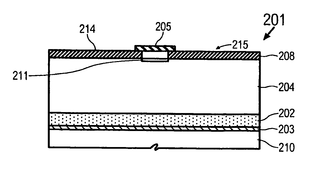
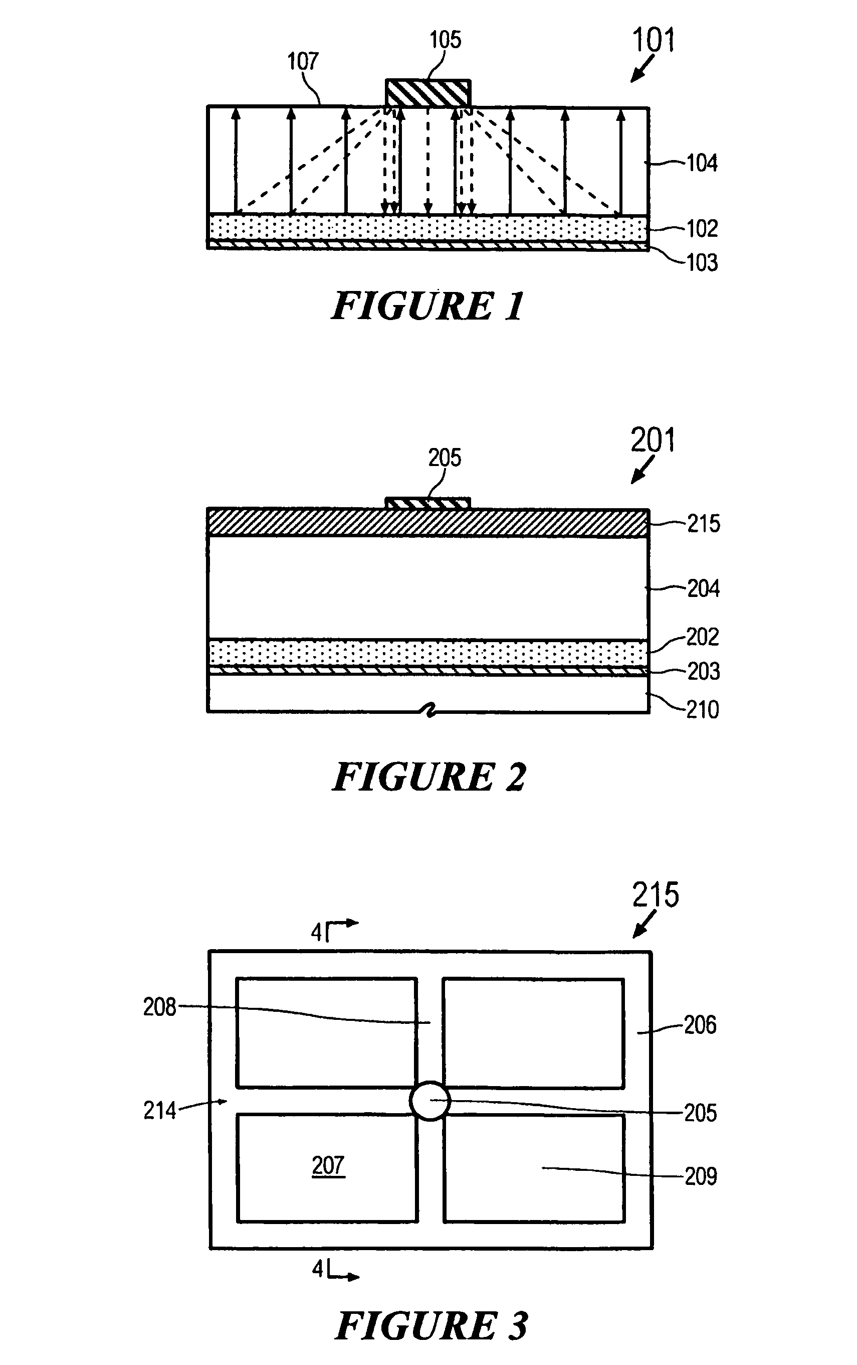
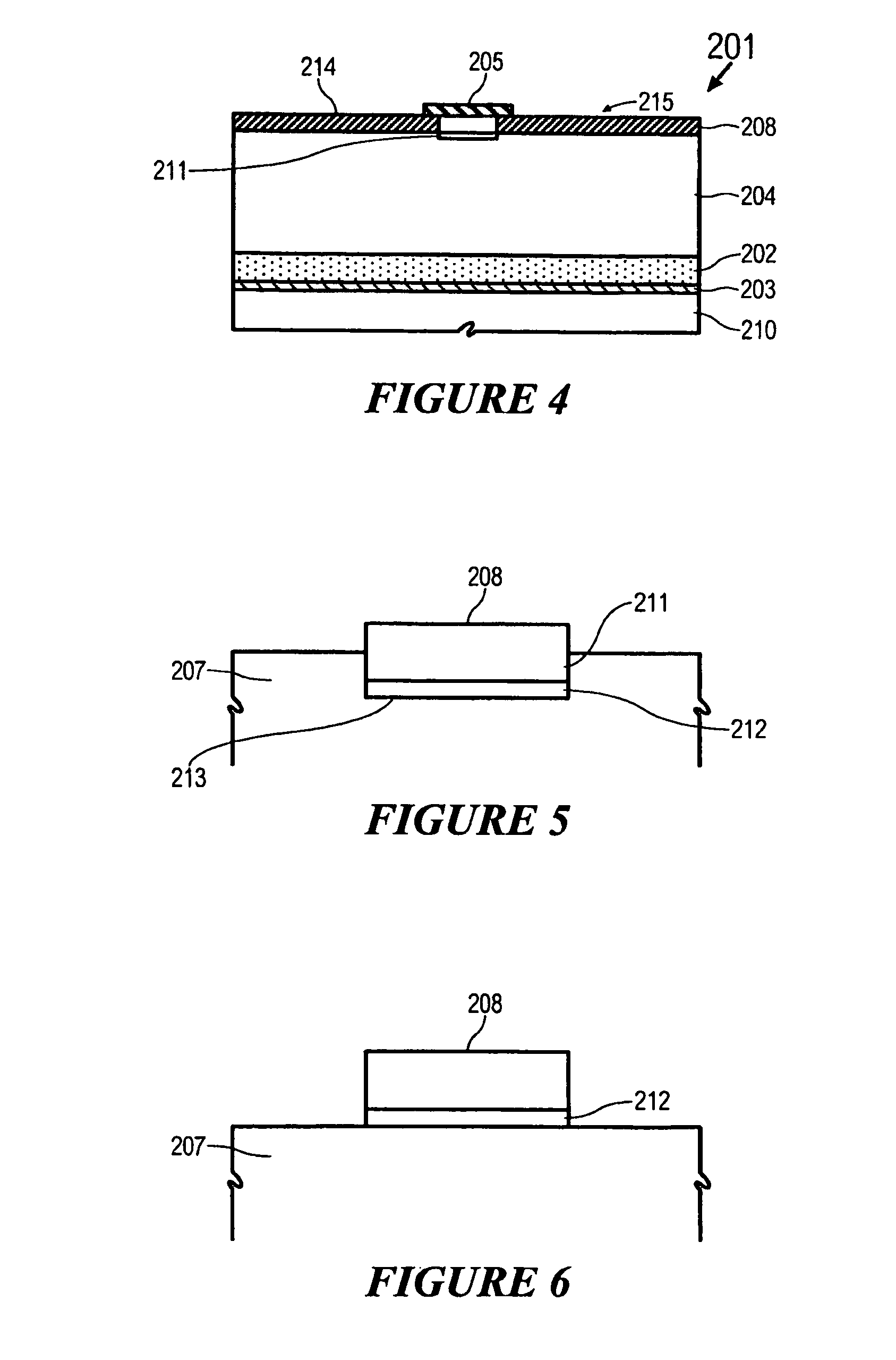
[0022]To first refer to FIG. 1 there is shown a light emitting device 101 such as, for example, a light emitting diode or a laser diode, and having a reflective layer and / or ohmic contact 103 on a first side of a plurality of epitaxial layers including an active region 102. A conductive metal layer 104 is on a second side of the epitaxial layers. The reflective layer 103 may be on the epitaxial layers and the ohmic contact on the reflective layer, or vice versa. There may be only one of them. A bonding pad 105 is provided on the light output surface 107. The electrical current flows in the metal layer 104 to the active layer 102 by the paths as shown with the dotted lines on FIG. 1. As can be seen, the maximum electrical current is concentrated under the bond pad 105. That means the maximum light emitted by the active layer 102 (as shown by the sold lines) will also be concentrated under the bonding pad 105. Such light will be reflected back into layer 104 by the bonding pad 105. Th...


PUM


Abstract

A light emitting device is disclosed that has a plurality of epitaxial layers including an active layer, at least one of a reflective layer and an ohmic contact on a first side of the epitaxial layers; and a layer of a conductive metal on a second side of the epitaxial layers and having a light emitting surface. A terminal is on the light emitting surface, the terminal comprising an array for diffusing electrical current and minimizing its effect on light output. The array may have a bonding pad, an outer portion, and a joining portion connecting the bonding pad and the outer portion; the outer portion and the joining portion being for current dissipation.

Description

CROSS REFERENCE TO RELATED APPLICATIONS[0001]This patent application is a U.S. National Phase application under 35 U.S.C. §371 of International Application No. PCT / SG2007 / 000288, filed on Sep. 4, 2007, entitled ELECTRICAL CURRENT DISTRIBUTION IN LIGHT EMITTING DEVICES, which claims priority to Singapore patent application number 200606050-3, filed Sep. 4, 2006.FIELD OF THE INVENTION[0002]This invention relates to electrical current distribution in light emitting devices and refers particularly, through not exclusively, to apparatus for spreading the electrical current so as to maximize light output.REFERENCE TO RELATED APPLICATION[0003]Reference is made to earlier Singapore patent application 200506301-1 filed 29 Sep. 2005, the contents of which are incorporated herein by reference as if disclosed herein in their entirely.BACKGROUD OF THE INVENTION[0004]In most light emitting devices such as for example, light emitting diodes and laser diodes, bonding pads occupy about 15% of the su...

Claims


Application Information

Patent Timeline
Patent Type & Authority Patents(United States)
IPC IPC(8): H01L33/00H01L21/00H01L33/38
CPCH01L33/38H01L24/97H01L33/20H01L2924/12041H01L2924/3011H01L2933/0016
Inventor YUAN, SHULIN, SHIMING
Owner TINGGI TECH PTE
Why Eureka
Try Eureka