Black level compensation circuit
a black level compensation and image sensor technology, applied in the field of analog blc circuits for image sensors, can solve the problems of leakage current and attenuation of the speed and accuracy of the conventional blc system, and achieve the effect of quick and accurate blc and saving chip area and power consumption
- Summary
- Abstract
- Description
- Claims
- Application Information
AI Technical Summary
Benefits of technology
Problems solved by technology
Method used
Image
Examples
first embodiment
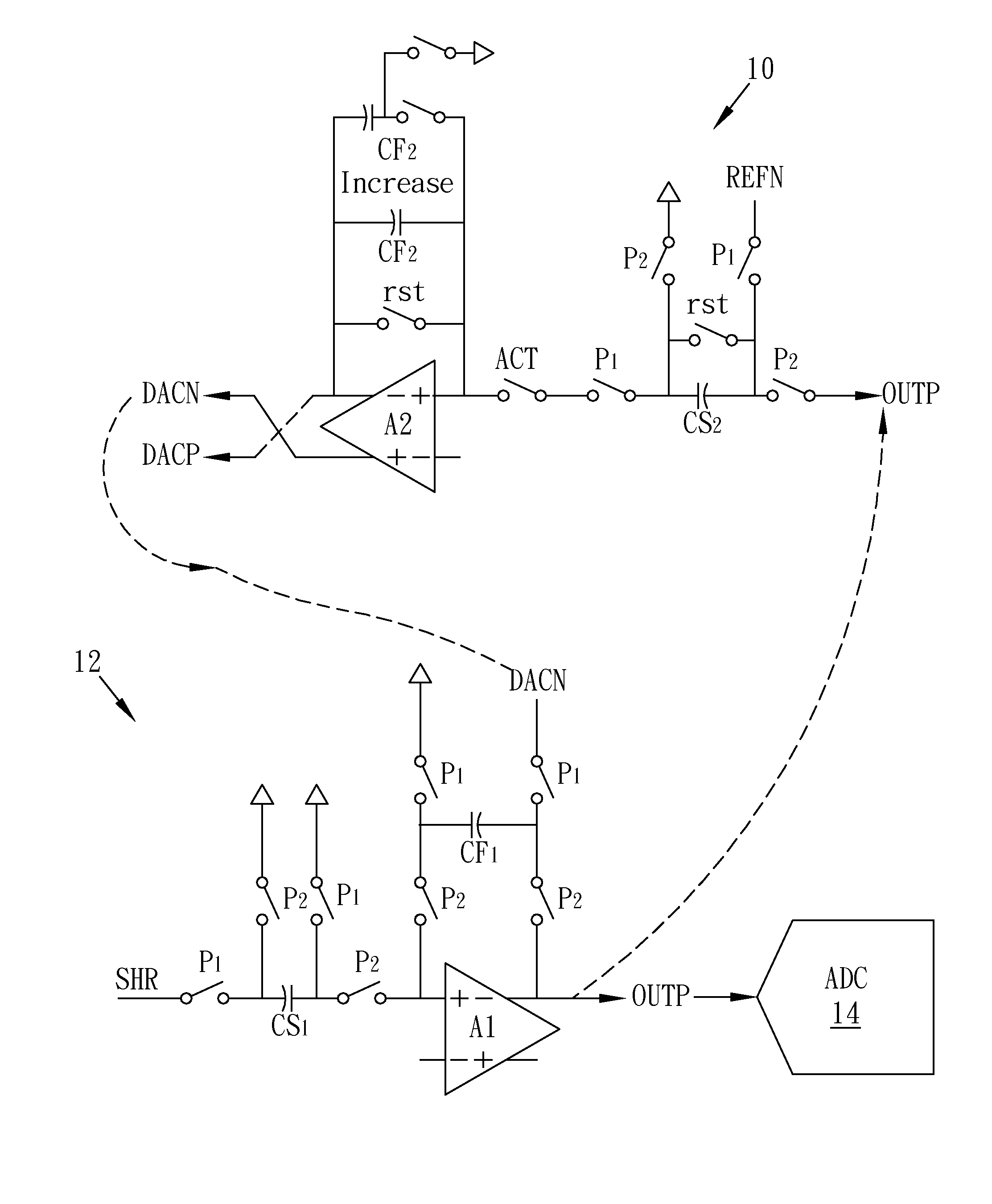
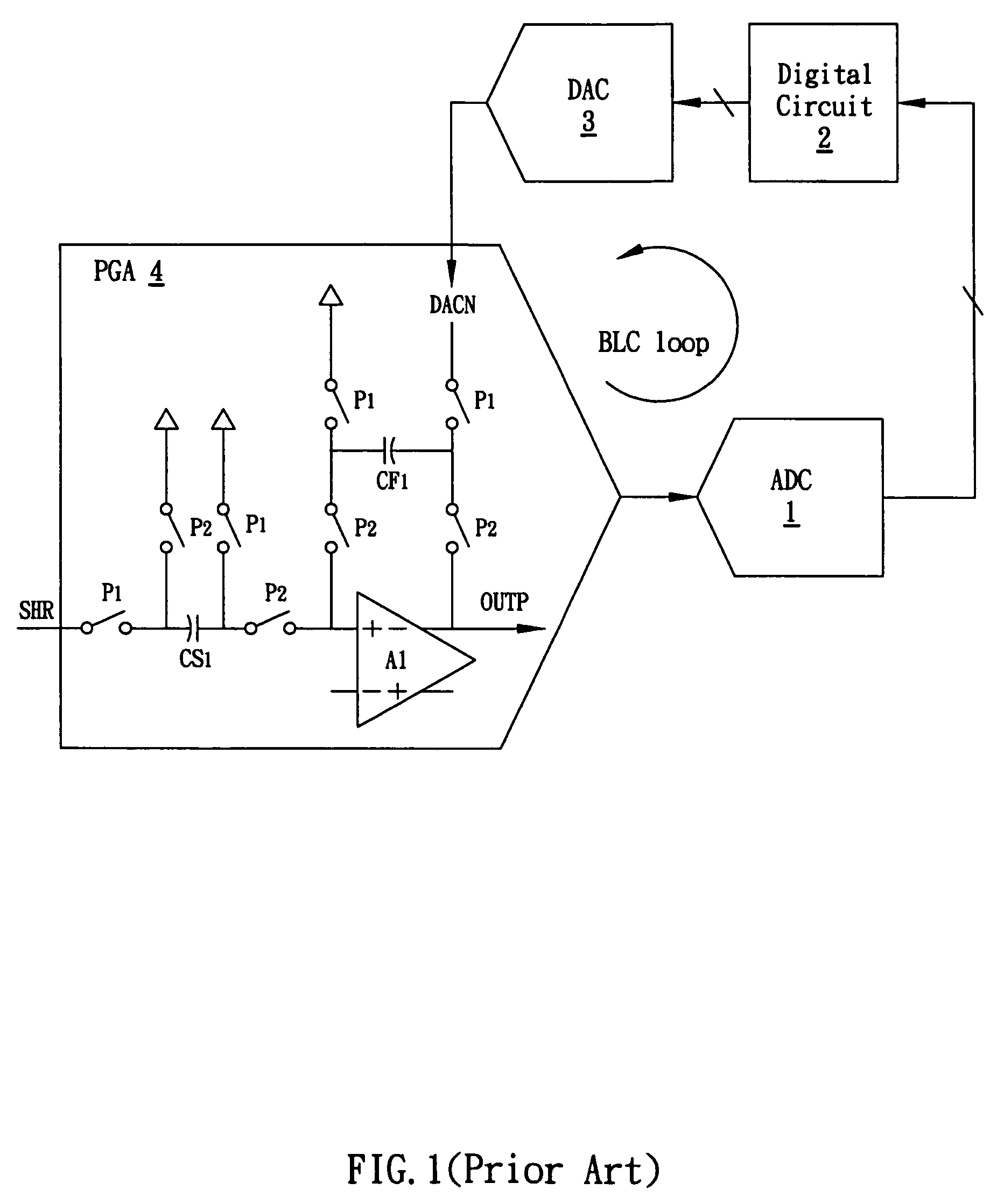
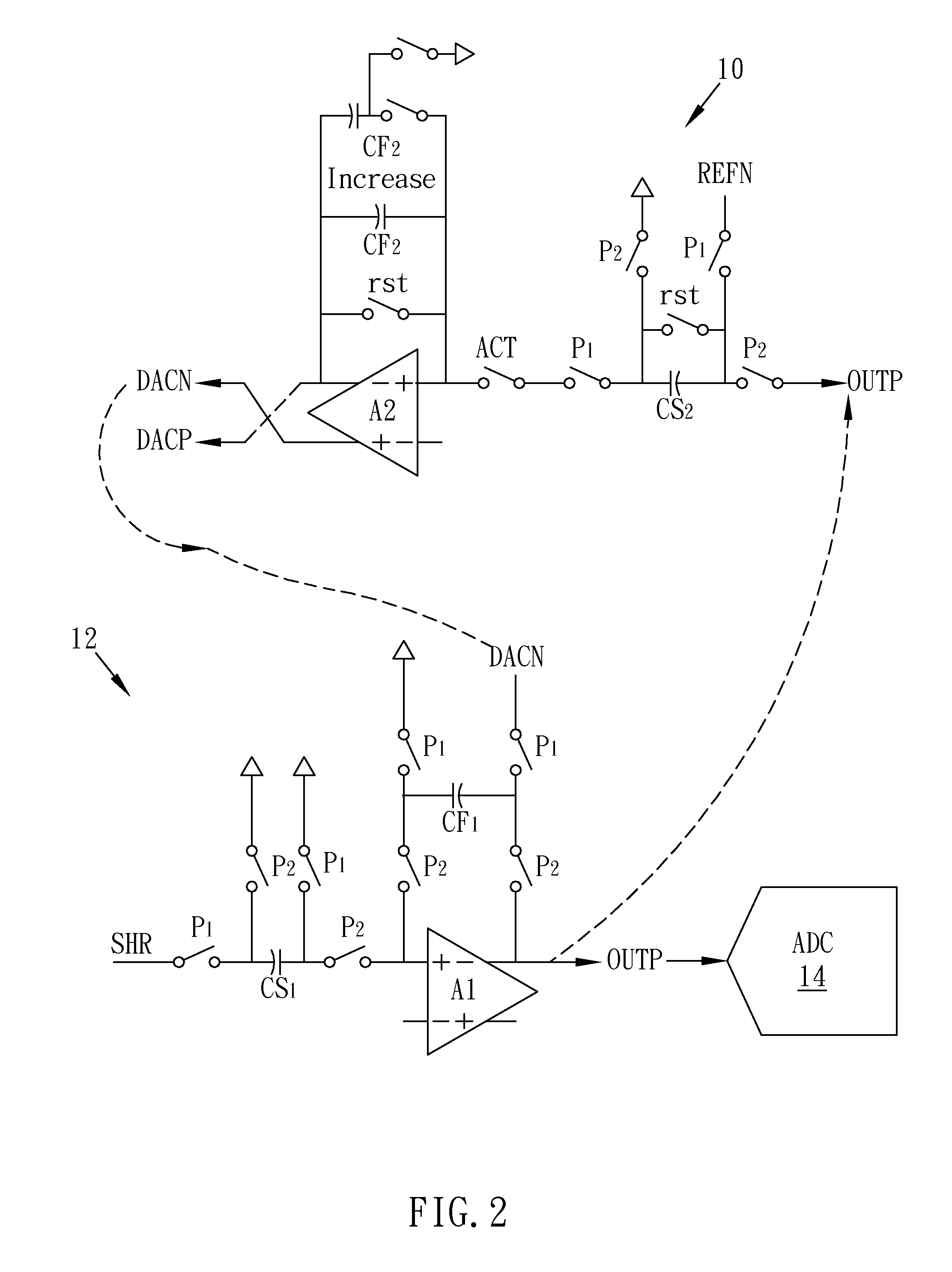
[0019]FIG. 2 shows a black level compensation (BLC) circuit, which is configured as a switched-capacitor (SC) integrator 10 and which is coupled to a readout amplifier according to the present invention. The BLC circuit 10 is used to compensate the readout amplifier, which comprises, for example, a programmable gain amplifier (PGA) 12 that amplifies signals obtained from an image sensor (not shown). An (open-loop) analog-to-digital converter (ADC) 14 receives the output of the PGA 12. In the embodiment, the output OUTP of the PGA 12 is connected to the input of the BLC circuit 10, and the (positive) output DACN of the BLC circuit 10 is controllably connected to charge a feedback capacitor CF1 or an input capacitor CS1 of the PGA 12, thereby forming a BLC loop, which is an analog loop rather than the digital loop used by the conventional BLC system (FIG. 1).
[0020]In the embodiment, the SC integrator 10 includes a compensation amplifier (e.g., a fully differential amplifier, which is ...
second embodiment
[0024]FIG. 4 shows a BLC circuit 10A / 10B according to the present invention. In the embodiment, a multi-stage (for example, two-stage) PGA 12A / 12B is applied. There is one BLC circuit corresponding to each PGA stage. For example, in one exemplary embodiment, the BLC circuit 10A is used to clamp the output of the PGA 12A, and the BLC circuit 10B is used to clamp the output of the PGA 12B. In another exemplary embodiment, however, only the final PGA stage is clamped while other stage or stages are ignored.
[0025]In the second embodiment (FIG. 4), the output voltage OUTP3 of the second-stage PGA 12B is clamped to the negative reference voltage REFN, and the output voltage OUTP of the first-stage PGA 12A is clamped to the voltage REFN / A3 (where A3=CS3 / CF3). Generally speaking, the target clamp voltage of each stage is scaled down with the ratio of the gain in the following PGA. For example, as shown in FIG. 4, the PGA gain A3 in the second stage is equal to CS3 / CF3, and the target clamp ...
PUM
 Abstract
Description
Claims
Application Information


