Laser diode and method of manufacturing the same

a technology of laser diodes and diodes, which is applied in the direction of lasers, laser construction details, semiconductor lasers, etc., can solve the problems of lowering the reliability of ultrasonics, high production costs, and inability to drive each ridge section independently, so as to achieve easy rotation and high production costs

Inactive Publication Date: 2012-03-06
SONY CORP
View PDF5 Cites 6 Cited by
  • Summary
  • Abstract
  • Description
  • Claims
  • Application Information

AI Technical Summary

Benefits of technology

[0005]However, in the case where the insulating material is embedded in the isolation trench, a stress is applied to the ridge section due to shrinkage and strain of the embedded insulating material, and a polarization angle of a laser beam radiated from the ridge section is easily rotated. Further, in the case where a deep isolation trench is formed, a step of embedding the insulating material becomes complicated, causing high production cost.
[0021]According to the first and the second methods of manufacturing a laser diode of the embodiments of the invention, the trench is formed between the ridge sections adjacent to each other. The wiring layer that electrically connects the upper cladding layer to the pad electrode is formed in the air at least over the trench by removing the sacrifice layer. Thus, there is no possibility that a stress generated in the case where a filler such as an insulating material is provided in the clearance between the wiring layer and the inner walls of the trench is not generated in the ridge section. Further, in the case where the foregoing wiring layer is formed by film formation, in the manufacturing process, there is no possibility that each wiring layer is contacted with each other, or reliability resulting from ultrasonic is lowered. Therefore, each ridge section is able to be driven independently, and rotation of a polarization angle resulting from the stress applied to the ridge section is able to be inhibited without lowering reliability.

Problems solved by technology

Further, in the case where a deep isolation trench is formed, a step of embedding the insulating material becomes complicated, causing high production cost.
However, in the case where the beam pitch is narrow as described above, one wire ball is contacted with a plurality of stripe electrodes, and each ridge section is not able to be driven independently.
Further, since ultrasonic bonding is used in wire bonding, there is a possibility that lowering of reliability resulting from ultrasonic is caused.
Accordingly, such a method is not able to be an effective means for solving the disadvantages.

Method used


Image

  • Laser diode and method of manufacturing the same
  • Laser diode and method of manufacturing the same
  • Laser diode and method of manufacturing the same

Examples


first embodiment

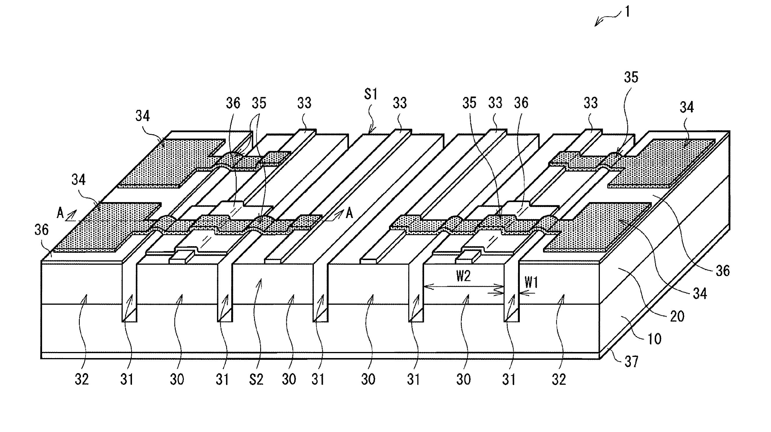
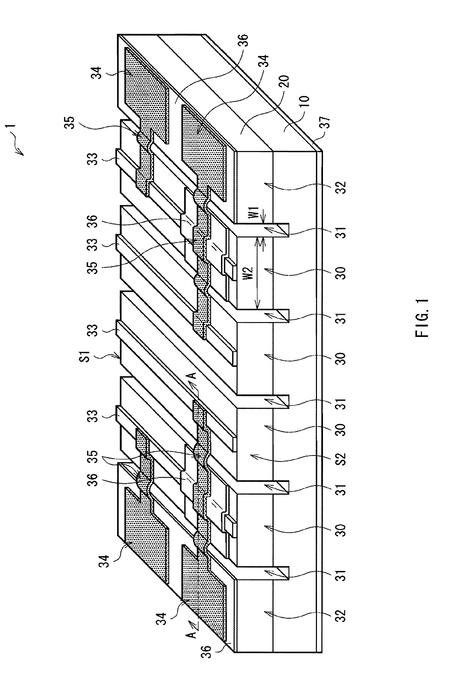
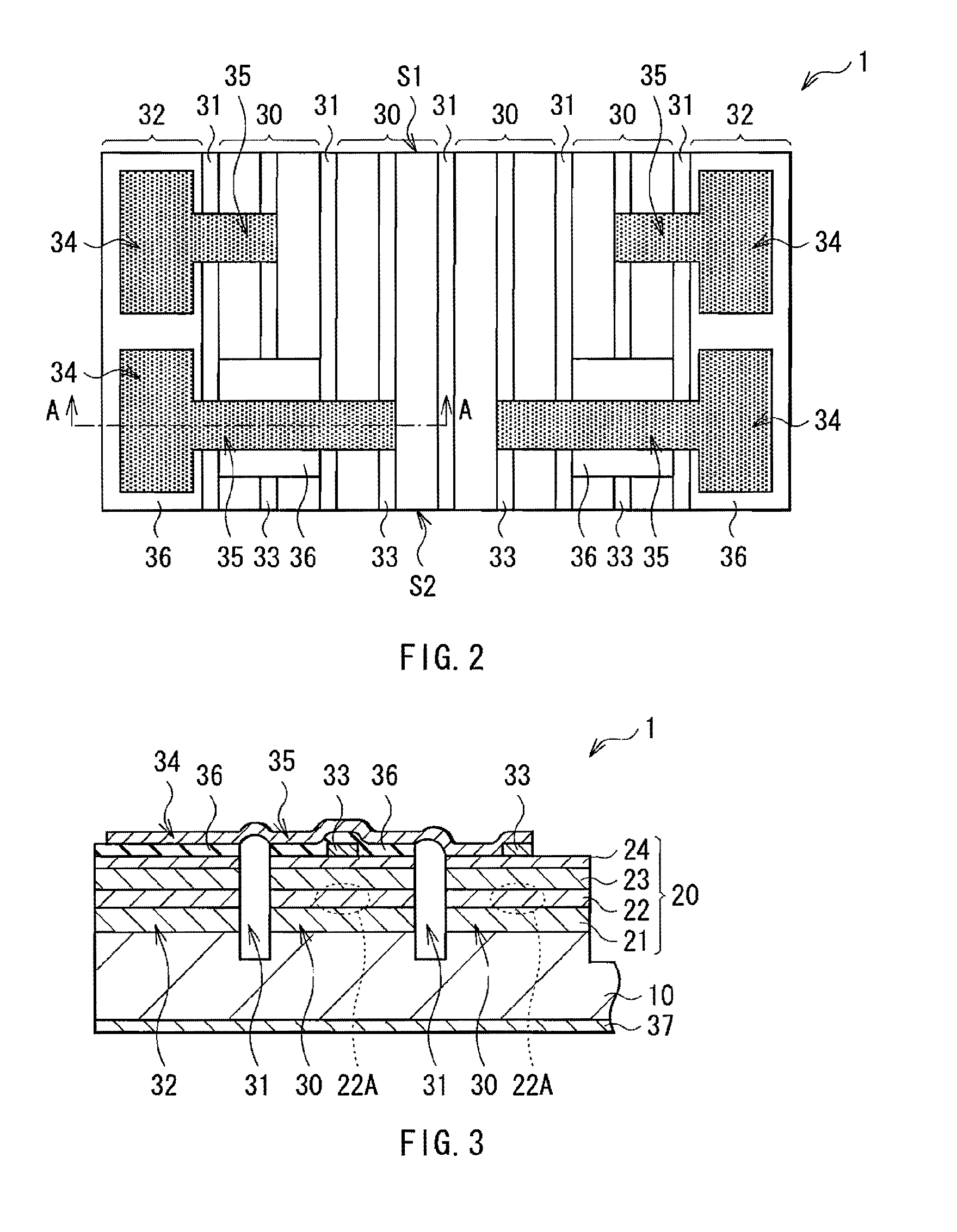
[0056]FIG. 1 is a perspective view illustrating an example of schematic structure of a laser diode 1 according to a first embodiment of the invention. FIG. 2 illustrates an example of top face structure of the laser diode 1 of FIG. 1. FIG. 3 illustrates an example of cross sectional structure taken along arrow A-A of the laser diode 1 of FIG. 1 or FIG. 2. The laser diode 1 according to this embodiment is a multibeam laser diode including a plurality of stripe-like emitters, and an edge emitting type laser diode in which a laser beam is radiated from an end face of each emitter.

[0057]The laser diode 1 of this embodiment includes, for example, a semiconductor layer 20 including a lower cladding layer 21, an active layer 22, an upper cladding layer 23, and a contact layer 24 in this order from the substrate 10 side over a substrate 10. Though not illustrated, the semiconductor layer 20 may be further provided with a layer other than the foregoing layers (for example, a buffer layer, a ...

second embodiment

[0078]FIG. 10 is a perspective view illustrating an example of schematic structure of a laser diode 2 according to a second embodiment of the invention. FIG. 11 illustrates an example of top face structure of the laser diode 2 of FIG. 10. FIG. 12 illustrates an example of cross sectional structure taken along arrow A-A of the laser diode 2 of FIG. 10 or FIG. 11.

[0079]The laser diode 2 according to this embodiment is a multibeam laser diode including a plurality of stripe-like emitters, and is an edge emitting type laser diode in which a laser beam is radiated from an end face of each emitter, as that of the foregoing embodiment is. What the laser diode 2 and the laser diode 1 of the foregoing embodiment have in common is that the laser diode 2 is formed by a method similar to that of the foregoing embodiment. However, the laser diode 2 is different from the laser diode 1 of the foregoing embodiment in that the all pad electrodes 34 are formed only in one region out of the two region...

modified example

[0093]In the foregoing respective embodiments, the wiring layer 35 is structured to overjump one trench 31 at a time. However, the wiring layer 35 may be structured to overjump a plurality of trenches 31 at a time. For example, as illustrated in FIG. 17, the wiring layer 35 may be structured to overjump two trenches 31 at a time. However, in this case, at least a section arranged in the air out of the wiring layer 35 is preferably in the shape of an arch.

[0094]Further, in the foregoing respective embodiments, the respective wiring layers 35 are configured of a single wiring. However, the wiring layer 35 may be configured of two or more fine wirings 35A that are arranged in parallel with each other with a given clearance in between. For example, as illustrated in FIG. 18, the respective wiring layers 35 may be configured of the two fine wirings 35A that are arranged in parallel with each other with a given clearance in between. Further, in the foregoing respective embodiments, the re...


PUM


Abstract

A laser diode capable of independently driving each ridge section, and inhibiting rotation of a polarization angle resulting from a stress applied to the ridge section without lowering reliability and a method of manufacturing the same are provided. A laser diode includes: three or more strip-like ridge sections in parallel with each other with a strip-like trench in between, including at least a lower cladding layer, an active layer, and an upper cladding layer in this order; an upper electrode on a top face of each ridge section, being electrically connected to the upper cladding layer; a wiring layer electrically connected to the upper electrode, in the air at least over the trench; and a pad electrode in a region different from regions of both the ridge section and the trench, being electrically connected to the upper electrode through the wiring layer.

Description

BACKGROUND OF THE INVENTION[0001]1. Field of the Invention[0002]The present invention relates to a laser diode capable of driving each emitter independently and a method of manufacturing the same.[0003]2. Description of the Related Art[0004]In a laser diode, in order to drive each emitter independently, an isolation trench to electrically isolate each emitter from an adjacent emitter is provided between emitters adjacent to each other. The width of the isolation trench varies according to the laser type. In the case of a narrow pitch type laser in which the beam pitch is about several tens of μm, the width of the isolation trench is only about several μm. Thus, in such a case, it is extremely difficult to provide a wiring layer that links a stripe electrode on the emitter (ridge section) with the both sides surrounded by the isolation trench, to a pad electrode formed in a location apart from the ridge section in the narrow isolation trench. Therefore, as described in Japanese Unexa...

Claims


Application Information

Patent Timeline
Patent Type & Authority Patents(United States)
IPC IPC(8): H01S5/00
CPCH01S5/4031H01S5/02276H01S5/0425H01S2301/176H01S2301/14H01S5/22H01S5/04256H01S5/02345
Inventor NAKASHIMA, MAKOTOYOKOYAMA, TAKAHIROKARINO, SACHIO
Owner SONY CORP
Why Eureka
Try Eureka