Electromechanical element, electric circuit device and production method of those

a technology of electric circuit device and electromechanical element, which is applied in the direction of electrostatic generator/motor, coating, generator/motor, etc., can solve the problems of reducing reliability and production of defective products, imposing a comparatively large mechanical load on the movable element, and reducing reliability or production of defective products. , to achieve the effect of preventing deformation and damage of the movable element, reducing the area and improving reliability

Inactive Publication Date: 2012-03-27
SONY CORP
View PDF11 Cites 42 Cited by
  • Summary
  • Abstract
  • Description
  • Claims
  • Application Information

AI Technical Summary

Benefits of technology

[0009]According to an electromechanical element, an electric circuit device and a method of fabricating the electromechanical element and the electric circuit device of embodiments of the present invention, effects on a movable element formed by etching the sacrifice layer, electrodes, or the like in the electromechanical element can be reduced, and the sacrifice layer can reliably be removed. The electromechanical element, an electric circuit device and a method of fabricating the electromechanical element and the electric circuit device according to embodiments of the present invention, improvement in the reliability and reduction in the occurrence rate of defective products can also be realized.
[0029]According to a method of fabricating an electromechanical element and an electric circuit device of embodiments of the present invention, since holes or through-holes are preliminary formed in the movable element of the electromechanical element, the sacrifice layer can be etched from a circumference of the movable element, as well as etching through the holes formed in the movable element. As a result, the sacrifice layer, particularly the central portion of the sacrifice layer can effectively and reliably be removed by etching.
[0031]As described above, according to an electromechanical element and an electric circuit device of embodiments of the present invention, since holes are formed in the movable element, not only can the sacrifice layer be etched from a circumference of the movable element, but the sacrifice layer can also be etched through the holes formed in the movable element. As a result, the sacrifice layer can reliably and rapidly be removed by etching to form the movable element having a large area, such as large-scale surface MEMS having more than 100 μm on a side. Further, since the holes are arranged in the movable element according to the above-described positional manner, pillar shaped or a wall shaped support portions for the movable element can be formed in the process of etching the sacrifice layer. Thus, since mechanical strength of the movable element can be maintained and deformation of and damage to the movable element can be prevented during the fabrication steps, reliability can be improved and defective products can be decreased.
[0032]According to a method of fabricating an electromechanical element and an electric circuit device according to embodiments of the present invention, the main etching is conducted without removing support portions that can mechanically support the movable element in the first etching step as described above. Therefore, deformation of or damage to the movable element can be prevented; for example, deformation due to mechanical load or damage to on the movable element caused by forming electrodes on the movable element can be prevented. As a result, reliability and a yield rate can be improved.
[0033]The hollow formed by selecting arrangement of the aforementioned holes in the first etching cannot be intercepted with the sacrifice layer remained as mechanical support portions in the second etching. Thus, corroding electrodes or the like with an etchant due to elongation of immersion time can also be prevented in the second etching.

Problems solved by technology

This may cause deformation of or damage to the movable element, thereby resulting in decrease in reliability and production of defective products.
However, the Al electrode is formed after removing the sacrifice layer by etching since the Al is corroded with a concentrated fluoric acid used as an etching solution for the sacrifice layer.
However, forming the Al electrode on the movable element floating in a hollow can impose a comparatively large mechanical load on the movable element, for example, the Al formation of entire surface, an entire surface coating of photoresist for forming a pattern with a required shape, and patterning by photolithography.
Such mechanical load on the movable element may cause deformation of or damage to the movable element, which may result in reduction in reliability or production of defective products.
Specifically, in a case in which the movable element includes a large area, accurately etching the sacrifice layer that is located under the movable element can be difficult when etching from a circumference to the center of the movable element.
Further, since etching may take a long time, etching after the formation of electrode mentioned above may impose some effects on the movable element.

Method used


Image

  • Electromechanical element, electric circuit device and production method of those
  • Electromechanical element, electric circuit device and production method of those
  • Electromechanical element, electric circuit device and production method of those

Examples


Embodiment Construction

[0056]Embodiments of an electromechanical element, an electric circuit device and a method of fabricating an electromechanical element and an electric circuit device are described with referring to drawings. However, the present invention is not limited to the embodiments.

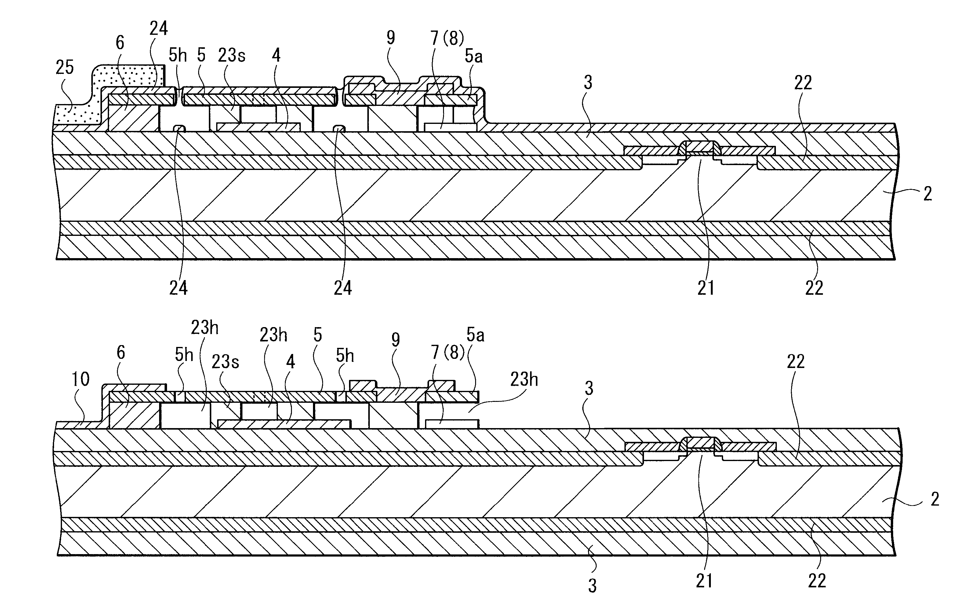
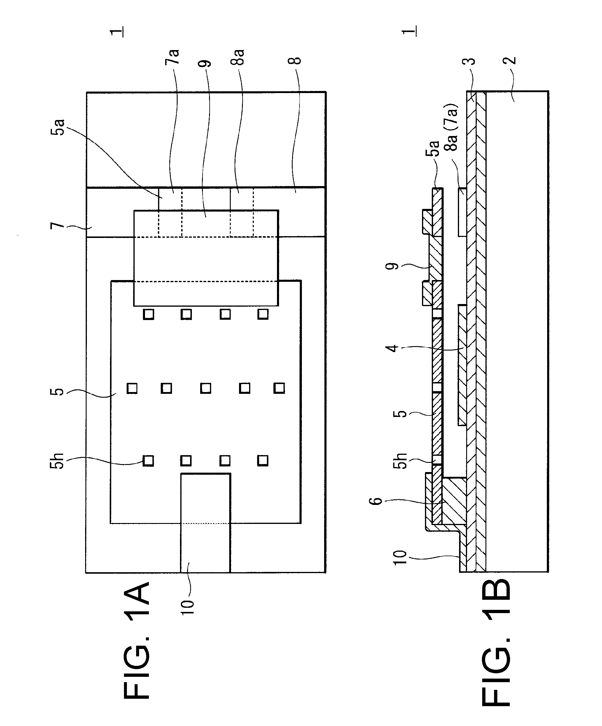
[0057]FIGS. 1A and 1B are schematic sectional views of an electromechanical element 1 according to an embodiment of the present invention.

[0058]The electromechanical element 1 indicates a switch element including an electrostatic actuator that turns on or off using an electrostatic drive.

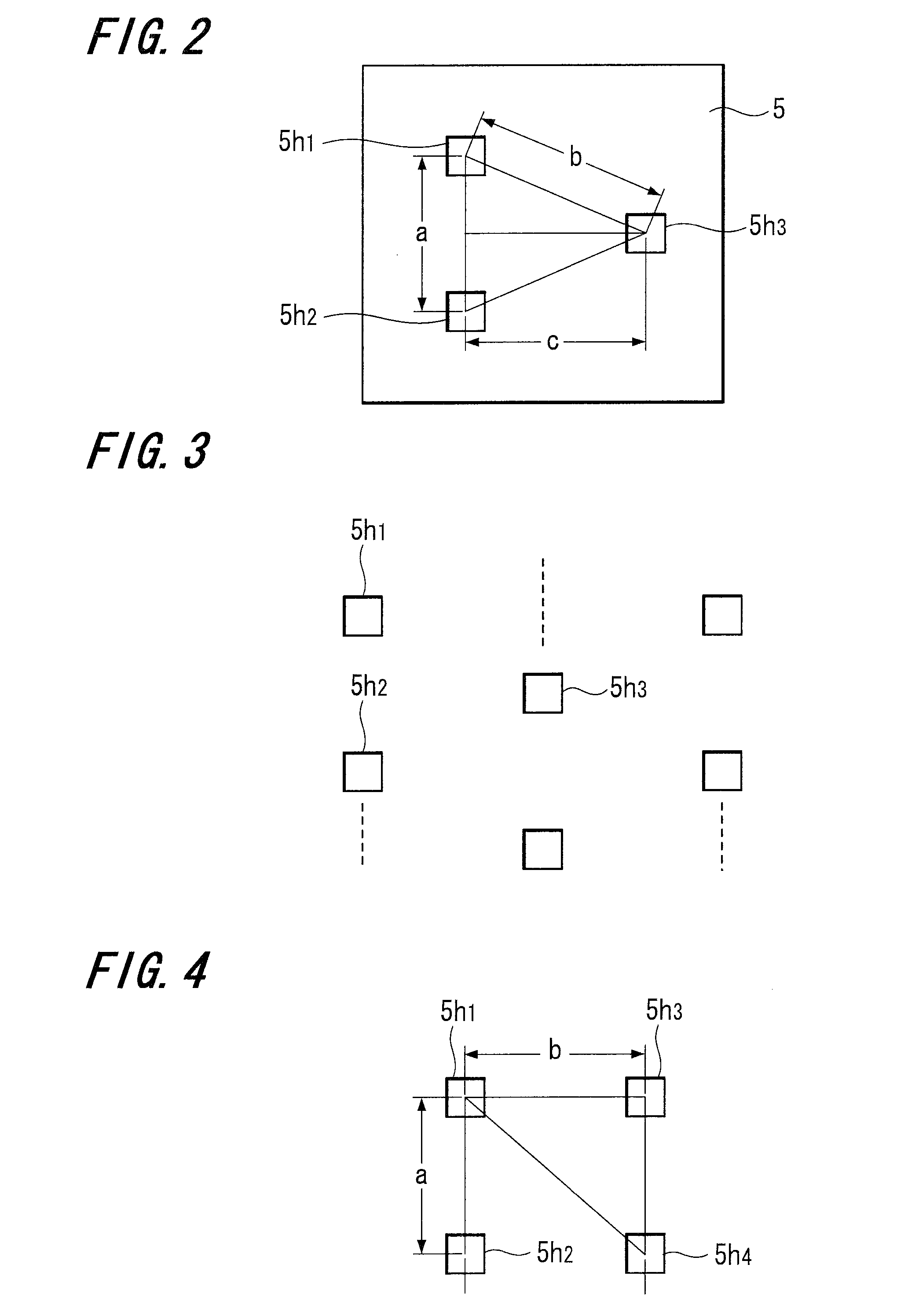
[0059]In the electromechanical element 1, specifically, in the electrostatic switch element, an insulating layer 3 is formed on a substrate 2, such as a crystal surface (100) forming a silicon semiconductor substrate surface, on which a fixed electrode 4 including an electrostatic actuator and a movable element 5 are formed, and the movable element 5, one end of which is fixed on the substrate 2 with an anchor 6 to form a cantileve...


PUM

PropertyMeasurementUnit
thicknessaaaaaaaaaa
thicknessaaaaaaaaaa
thicknessaaaaaaaaaa

Abstract

An electromechanical element includes a mechanically movable element through a hollow formed on a substrate, and a plurality of holes formed in the movable element. In the electromechanical element, the plurality of holes are arranged such that at least two holes are in a same line, at least one hole is in another line located adjacent to the one line with at least two holes, and a distance between one of the holes arranged in the same line and the other hole located at the closest position from the one of the two holes arranged in the same line is longer than a distance between the holes adjacently arranged in the same line.

Description

CROSS REFERENCES TO RELATED APPLICATIONS[0001]The present invention contains subject manner related to Japanese Patent Application JP 2006-042987 filed in the Japanese Patent Office on Feb. 20, 2006, the entire contents of which being incorporated herein by reference.BACKGROUND OF THE INVENTION[0002]1. Field of the Invention[0003]The present invention relates to an electromechanical element, an electric circuit device and a method of fabricating the electromechanical element and the electric circuit device.[0004]2. Description of the Related Art[0005]A micro electromechanical element, or MEMS (Micro Electro Mechanical System) is used as a single element for a switch, filter and capacitor or the like, or installed on a common semiconductor substrate with a circuit element of another semiconductor elements or the like to form various electric circuit devices (e.g., see patent publication: Japanese Unexamined patent publication H9-162462).[0006]The MEMS includes a movable element, or a...

Claims


Application Information

Patent Timeline
Patent Type & Authority Patents(United States)
IPC IPC(8): H01L21/302B81C1/00
CPCB81C1/00896B81B2207/015B81C2201/056
Inventor AKIBA, AKIRAMITARAI, SHUN
Owner SONY CORP
Why Eureka
Try Eureka