

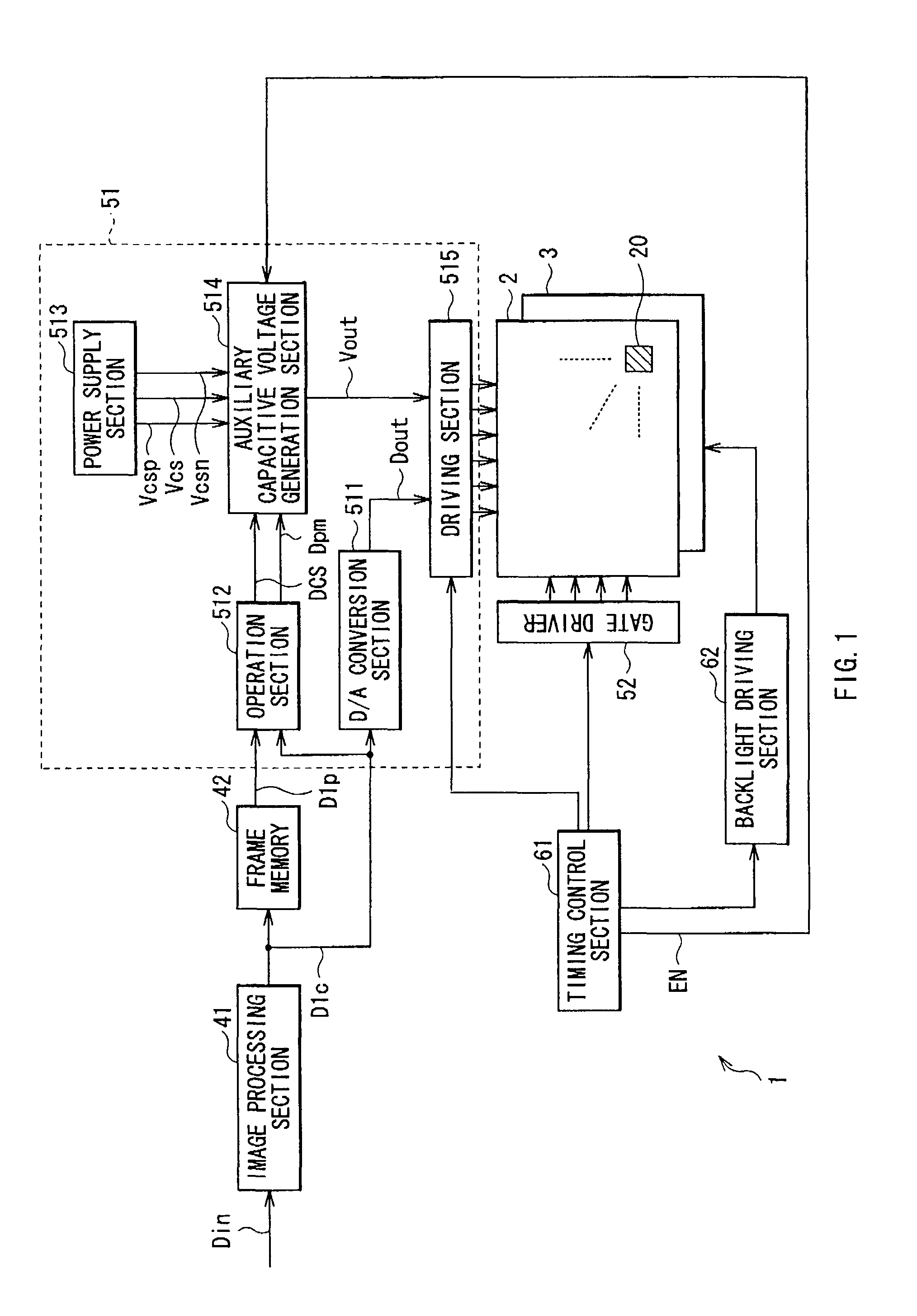
Image display device, display panel and method of driving image display device
a technology of image display device and display panel, which is applied in the direction of instruments, static indicating devices, etc., can solve the problems of deteriorating the reliability of the driving element, increasing power consumption and heating value, and low response speed
- Summary
- Abstract
- Description
- Claims
- Application Information
AI Technical Summary
Benefits of technology
Problems solved by technology
Method used
Image

Examples
first modification
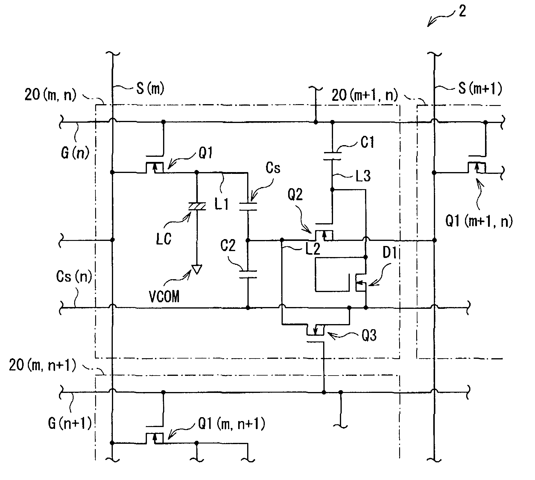
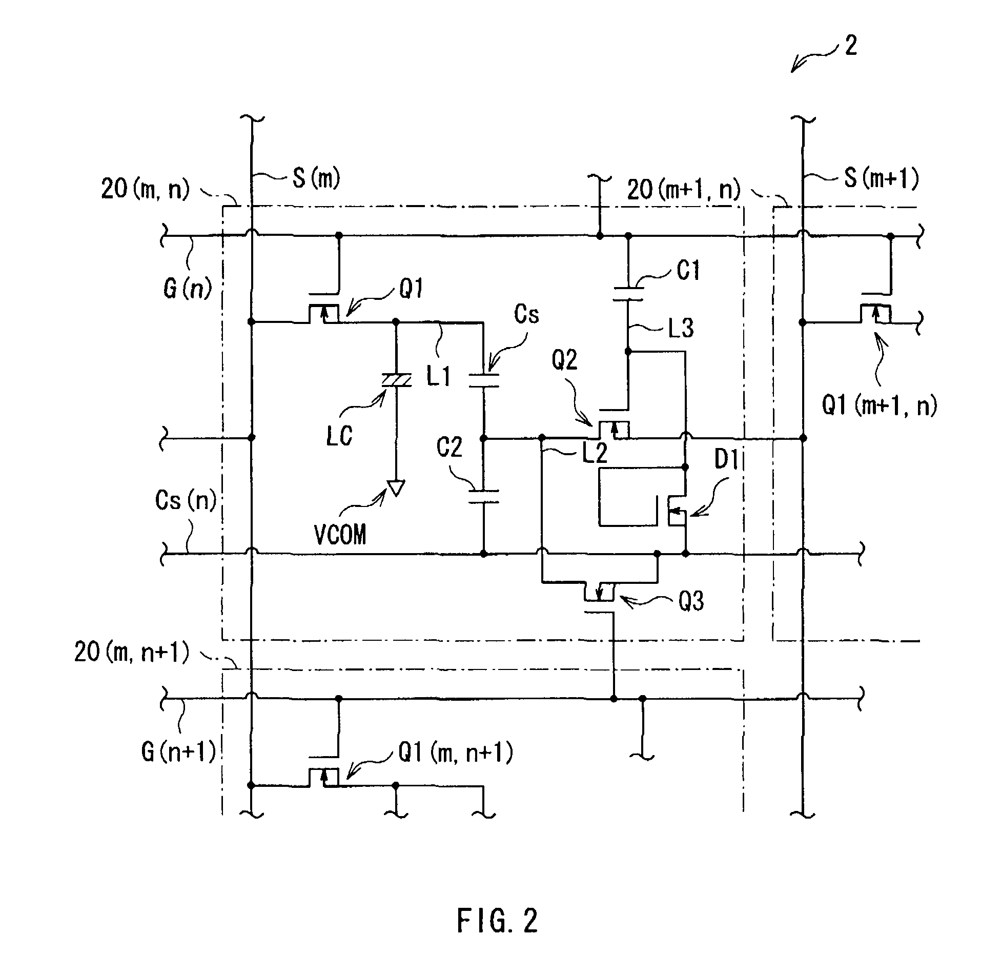
[0090]FIG. 12 shows the circuit configuration of a pixel circuit unit formed in an individual pixel 21 of a display panel (a liquid crystal display panel 2A) according to a first modification. FIG. 13 shows the driving operation of the pixel circuit unit according to the first modification by a timing waveform diagram (timings t10 to t19).
[0091]The pixel circuit unit within the pixel 21 (m, n) in the first modification is similar to the pixel 20 (m, n) in the foregoing embodiment, except that the gate line is composed of two gate lines, namely a gate line (the main gate line) G(n) and an auxiliary gate line Ga(n), and therefore neither the capacitive element C1 nor the diode D1 is disposed.
[0092]Specifically, the gate of a transistor Q2 of the first modification is connected via a connection line L4 to the auxiliary gate line Ga(n), the source thereof is connected to a source line S(m+1), and the drain thereof is connected via a connection line L2 to the opposite electrode of an aux...
second modification
[0095]FIG. 14 shows the circuit configuration of a pixel circuit unit formed in an individual pixel 22 of a display panel (a liquid crystal display panel 2B) according to a second modification. FIG. 15 shows the driving operation of the pixel circuit unit according to the second modification by a timing waveform diagram (timings t20 to t28).
[0096]The pixel circuit unit within the pixel 22 (m, n) in the second modification is similar to the pixel 20 (m, n) in the foregoing embodiment, except that the gate line is composed of two gate lines, namely a gate line (the main gate line) G(n) and an auxiliary gate line Ga(n), and therefore, the capacitive element C2 is not disposed.
[0097]Specifically, the gate of a transistor Q3 of the second modification is connected to the auxiliary gate line Ga(n), the source thereof is connected to an auxiliary capacitive line Cs(n), and the drain thereof is connected via a connection line L2 to the opposite electrode of an auxiliary capacitive element C...
third modification
[0100]FIG. 16 shows the circuit configuration of a pixel circuit unit formed in an individual pixel 23 of a display panel (a liquid crystal display panel 2C) according to a third modification. FIG. 17 shows the driving operation of the pixel circuit unit according to the third modification by a timing waveform diagram (timings t30 to t37).
[0101]The pixel circuit unit within the pixel 23 (m, n) in the third modification is similar to the pixel 20 (m, n) in the foregoing embodiment, except that the source line is composed of two source lines, namely a source line (the main source line) S(m) and an auxiliary source line Sa(m), and therefore neither the capacitive element C1 nor the diode D1 is disposed.
[0102]Specifically, the gate of a transistor Q2 of the third modification is connected via a connection line L4 to the gate line G (n), the source thereof is connected to the auxiliary source line Sa(m), and the drain thereof is connected via a connection line L2 to the opposite electrod...
PUM
 Abstract
Description
Claims
Application Information