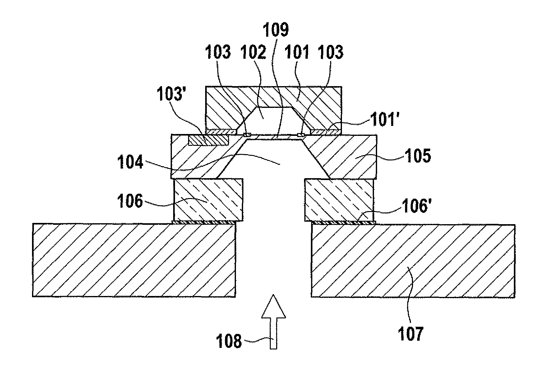
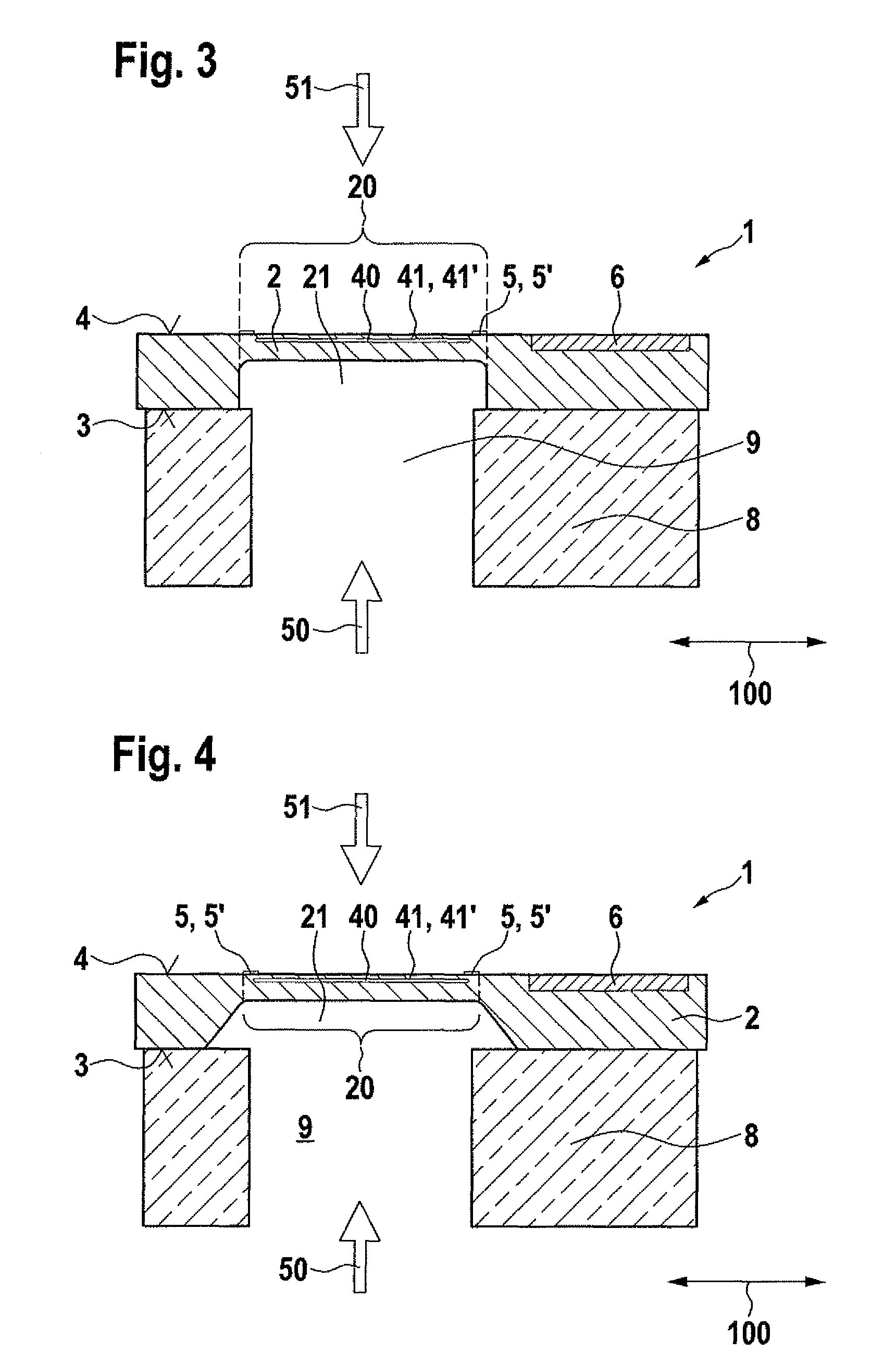
[0002]The sensor system according to the present invention and the method according to the present invention for manufacturing a sensor system have the advantage over the related art that mechanical decoupling of the diaphragm area from a second pressure on the second side of the substrate is achieved. This is accomplished in that the decoupling element is introduced into the material of the diaphragm area. A pressure variation of the second pressure thus does not result in a deflection movement of the diaphragm area perpendicularly to the main extension plane, but rather is instead absorbed by the decoupling element. A deflection movement of the diaphragm area perpendicularly to the main extension plane is advantageously exclusively caused by a variation of a first pressure in the trench, so that a detected deflection movement is uniquely to be assigned to this first pressure. The sensor system is thus usable as an absolute pressure sensor. The measuring precision of the sensor system is further increased overall and the impairment of the measuring precision by variations of the second pressure is reduced. Advantageously, a further absolute pressure sensor or a further reference volume is thus not required, so that costly capping of the sensor system or the second side of the substrate may be dispensed with. The integration of the decoupling element in the diaphragm area further allows implementing a comparatively compact installation, and cost-effective manufacturing of the sensor system. The substrate preferably includes a semiconductor substrate and particularly preferably a silicon substrate.
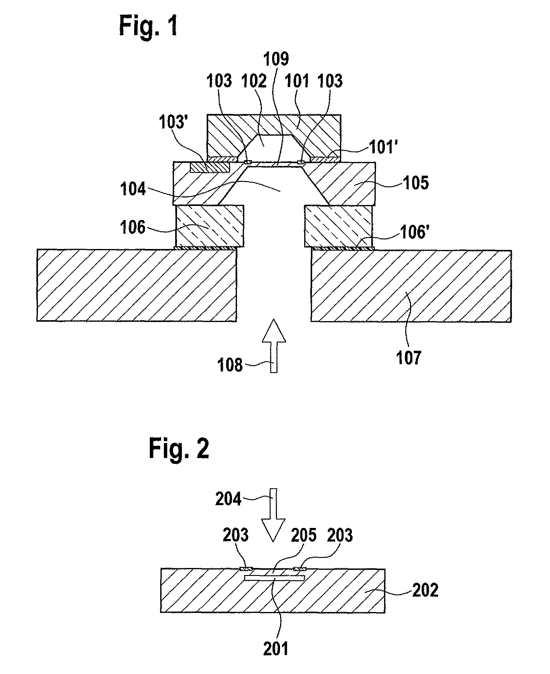
[0003]According to a preferred specific embodiment, it is provided that the decoupling element includes a cavern, the cavern preferably being smaller along the main extension plane than the diaphragm area and / or the diaphragm area having a further diaphragm area in the area of the cavern. A comparatively cost-effective implementation of a decoupling element is thus advantageously implemented. A pressure variation of the second pressure is absorbed by a decoupling movement of the further diaphragm area perpendicularly to the main extension plane, so that the action of a force on the diaphragm area perpendicularly to the main extension plane is prevented. A vacuum, which damps the decoupling movement in the desired manner, is preferably hermetically enclosed inside the cavern. The further diaphragm area has a lower material thickness in comparison to the diaphragm area, in particular perpendicularly to the main extension plane. The further diaphragm area preferably includes an APSM diaphragm (advanced porous silicon membrane). The diaphragm area and / or the further diaphragm area include a round or polygonal, preferably square cross-section parallel to the main extension plane in particular.
[0006]According to a preferred specific embodiment, it is provided that the trench is provided extending essentially perpendicularly to the main extension plane from the first side up to the first diaphragm area. The sensor system thus advantageously has a comparatively high media resistance, because the first pressure to be measured is supplied to the diaphragm area through the trench from the first side of the substrate, in particular the rear side of the substrate, so that a pressure measurement of aggressive media is advantageously achievable.
[0008]A further object of the present invention is a method for manufacturing a sensor system, the substrate being provided in a first manufacturing step, the decoupling element being manufactured in a second manufacturing step, and the trench being manufactured in a third manufacturing step. The sensor system is thus producible comparatively cost-effectively, standard micromechanical manufacturing methods (preferably in surface micromechanics), for example, in 200 mm technology, being usable in particular.
[0009]According to a preferred specific embodiment, it is provided that in a fourth manufacturing step, the detection elements and / or the analysis circuit are placed in the area of the second side. The detection elements and / or the analysis circuit may advantageously be manufactured cost-effectively and using a comparatively compact installation space in standard semiconductor manufacturing methods.

