Electromagnectic wave detecting element

a technology of electromagnetic waves and elements, applied in the direction of electrical equipment, semiconductor devices, radio frequency control devices, etc., to prevent the reduction of the efficiency of utilizing electromagnetic waves at the sensor portion

Active Publication Date: 2012-05-08
FUJIFILM CORP
View PDF8 Cites 3 Cited by
  • Summary
  • Abstract
  • Description
  • Claims
  • Application Information

AI Technical Summary

Benefits of technology

[0016]The present invention provides an electromagnetic wave detecting element that, although equipped with a common electrode line, can prevent a decrease in the efficiency of utilizing electromagnetic waves at sensor portions.
[0020]In this way, in the electromagnetic wave detecting element of the present invention of the above-described aspect, the common electrode line that supplies bias voltage to the first electrodes is formed further toward the downstream side of the electromagnetic waves than the sensor portions. Accordingly, shielding of the electromagnetic waves, that are irradiated onto the semiconductor layer, by the common electrode line is eliminated. Therefore, even though the electromagnetic wave detecting element of the present invention of the above-described aspect is provided with a common electrode line, it can prevent a decrease in the efficiency of utilizing electromagnetic waves at the sensor portions.
[0021]In a second aspect of the present invention, in the above-described aspect, the common electrode line may have low resistance compared to the electrically-conductive members that form the first electrodes.
[0035]In this way, in accordance with the present invention, the common electrode line, that supplies bias voltage to the first electrodes and that is formed from a light-shielding, low-resistance wiring material, is formed at the electromagnetic wave downstream side of the sensor portions. Accordingly, an electromagnetic wave detecting element can be provided that, although equipped with a common electrode line, can prevent a decrease in the efficiency of utilizing electromagnetic waves at sensor portions.

Problems solved by technology

However, such problems arise as well in cases in which the object of detection is any type of electromagnetic waves such as ultraviolet rays or infrared rays.

Method used


Image

  • Electromagnectic wave detecting element
  • Electromagnectic wave detecting element
  • Electromagnectic wave detecting element

Examples


first exemplary embodiment

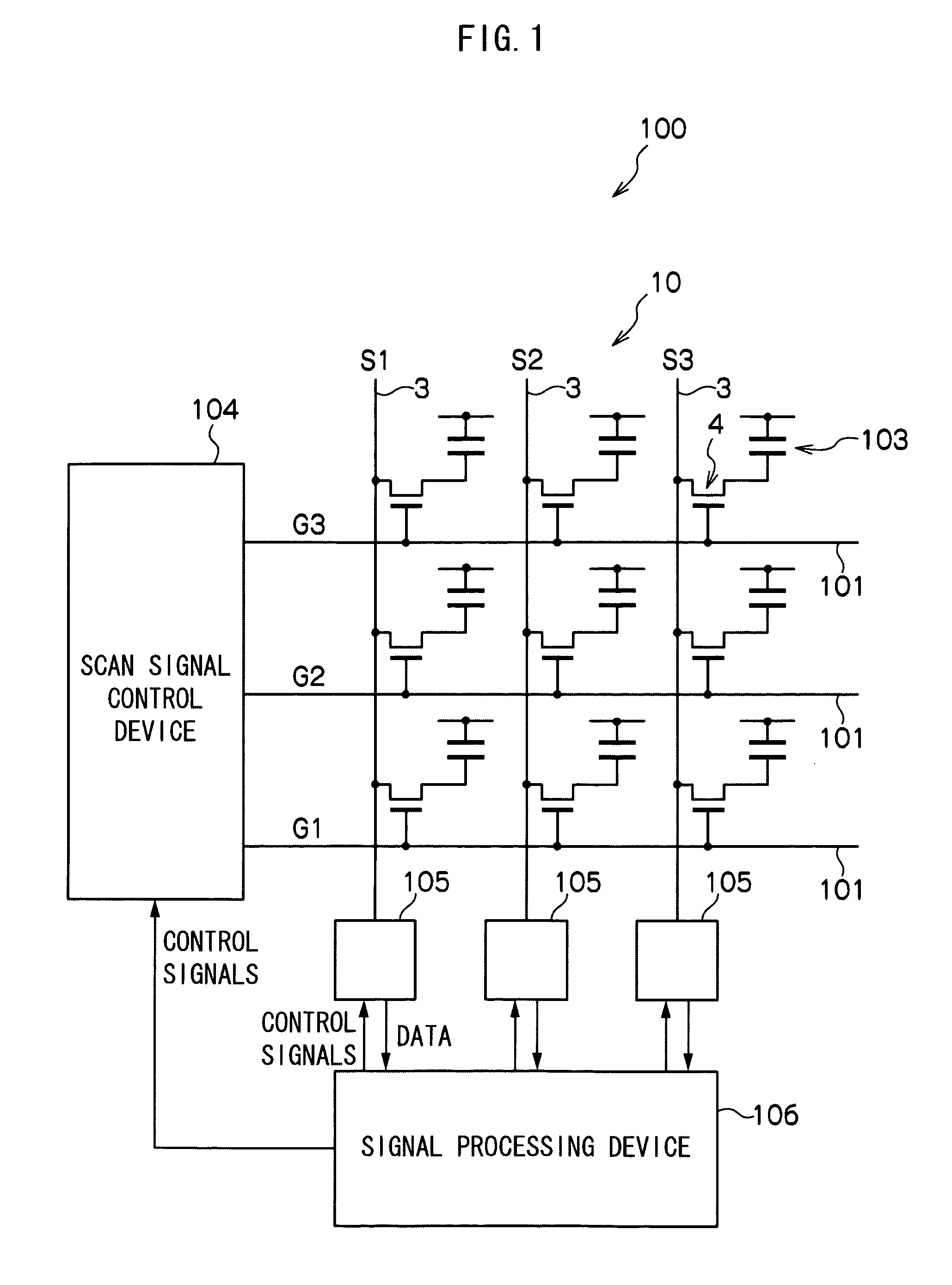
[0058]The overall structure of the radiation image detection device 100 relating to a first exemplary embodiment is illustrated in FIG. 1. However, a scintillator that converts radiation into light is not illustrated.

[0059]As shown in FIG. 1, the radiation image detection device 100 relating to the present exemplary embodiment has an electromagnetic wave detecting element 10.

[0060]The electromagnetic wave detecting element 10 has upper electrode, semiconductor layer, and lower electrode that will be described later. A large number of pixels that are structured to include sensor portions 103 and TFT switches 4 are provided in a two-dimensional form at the electromagnetic wave detecting element 10. The sensor portion 103 receives light, that is obtained by irradiated radiation being converted at a scintillator, and accumulates charges. The TFT switch 4 reads-out the charges accumulated in the sensor portion 103.

[0061]Plural scan lines 101 for turning the TFT switches 4 on and off, and...

second exemplary embodiment

[0098]In a case in which different types of lines are formed at the same wiring layer in the electromagnetic wave detecting element 10, it is easy for leaks to arise between the lines due to poor patterning.

[0099]Thus, a second exemplary embodiment describes a case in which the scan lines 101, the signal lines 3, and the common electrode lines 25 are formed by different wiring layers.

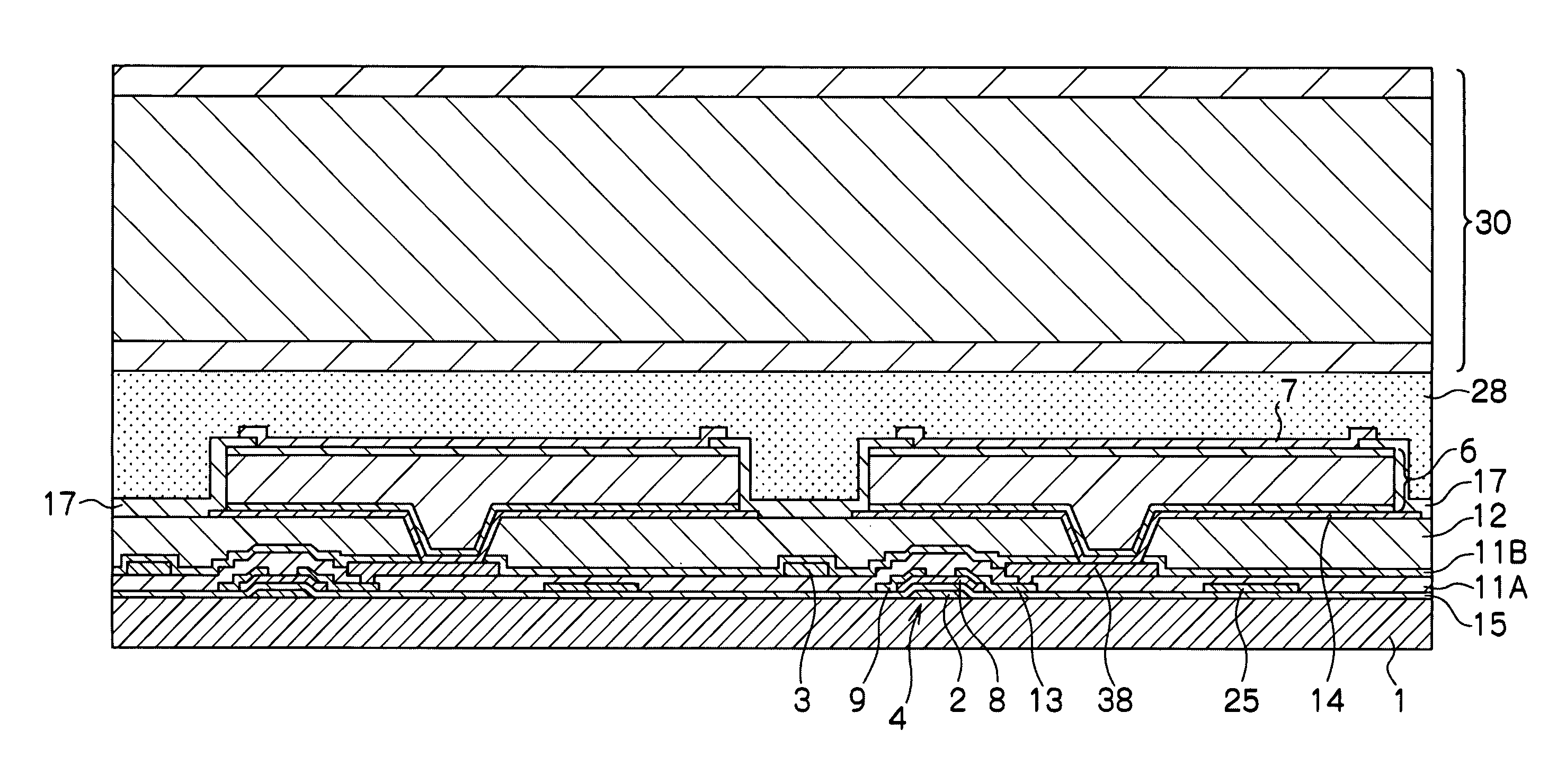
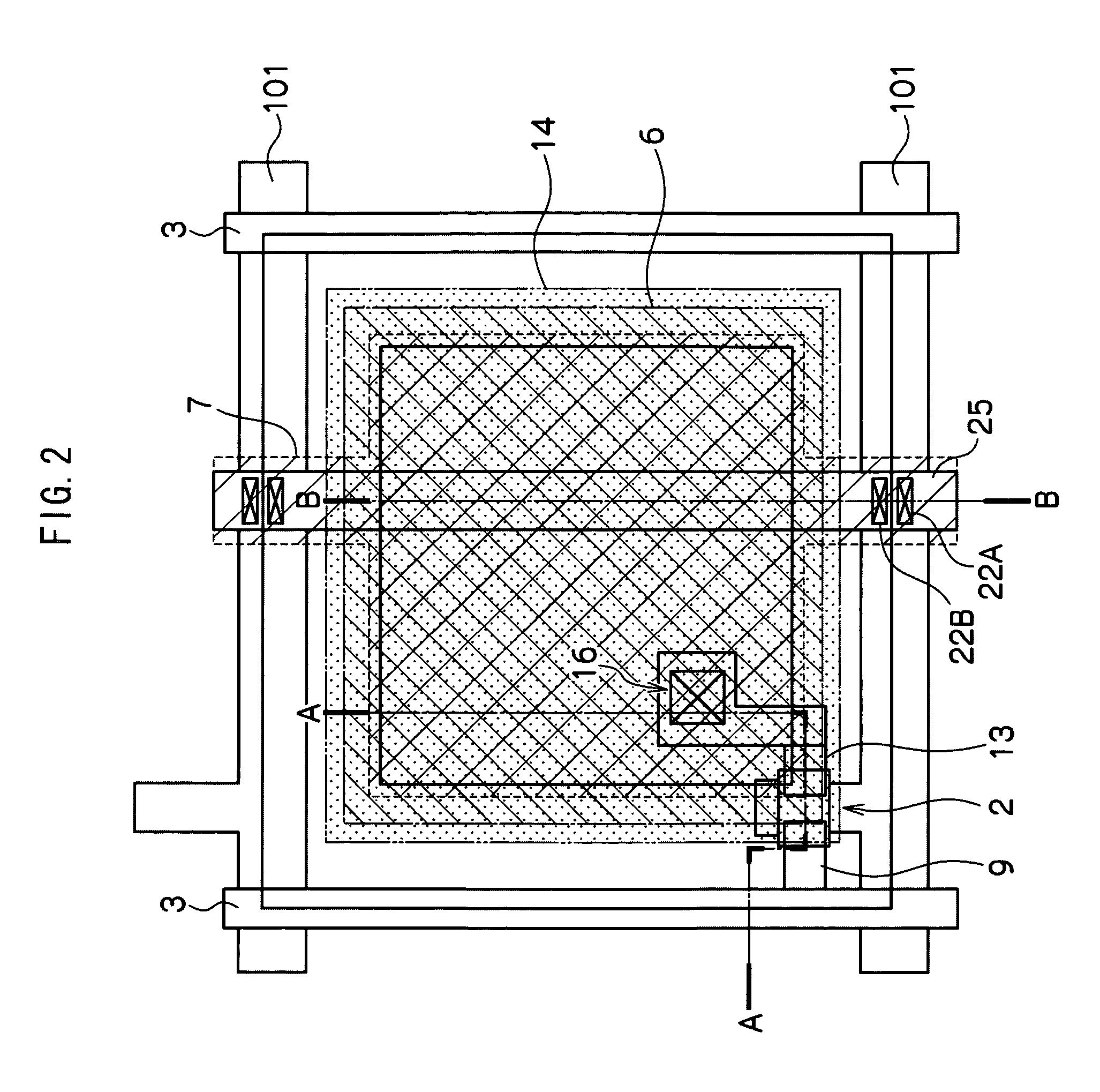
[0100]A plan view showing the structure of one pixel unit of the electromagnetic wave detecting element 10 relating to the second exemplary embodiment is shown in FIG. 6. Further, a cross-sectional view along line A-A of FIG. 6 is shown in FIG. 7A, and a cross-sectional view along line B-B of FIG. 6 is shown in FIG. 7B. Description of portions in FIG. 6 and FIG. 7, that are the same as in FIG. 2 and FIG. 3, is omitted.

[0101]As shown in FIG. 7A and FIG. 7B, at the electromagnetic wave detecting element 10, the scan line 101 and the gate electrode 2 are formed on the substrate 1, and the scan line 101 and...

third exemplary embodiment

[0122]In the first and second exemplary embodiments, the connection regions of the upper electrodes 7 and the common electrode lines 25 are formed on the protective insulating film 17. However, there are cases in which disconnection or the like of the connection regions arises due to changes in the steep angle of the protective insulating film 17 at the lower layer, or cracking, or the like.

[0123]Thus, the third exemplary embodiment describes a case in which an interlayer insulating film 18 is further formed at the peripheries of the respective semiconductor layer 6.

[0124]A plan view showing the structure of one pixel unit of the electromagnetic wave detecting element 10 relating to the third exemplary embodiment is shown in FIG. 17. Further, a cross-sectional view along line A-A of FIG. 17 is shown in FIG. 18A, and a cross-sectional view along line B-B of FIG. 17 is shown in FIG. 18B. Descriptions of portions in FIG. 17 and FIG. 18, that are the same as in FIG. 2 and FIG. 3, are om...


PUM


Abstract

The present invention is to provide an electromagnetic wave detecting element that can prevent a decrease in light utilization efficiency at sensor portions. The sensor portions are provided so as to correspond to respective intersection portions of scan lines and signal lines, and have semiconductor layer that generate charges due to electromagnetic waves being irradiated, and at whose electromagnetic wave irradiation surface sides upper electrodes are formed, and at whose electromagnetic wave non-irradiation surface sides lower electrodes are formed. Bias voltage is supplied to the respective upper electrodes via respective contact holes by a common electrode line that is formed further toward an electromagnetic wave downstream side than the semiconductor layer.

Description

CROSS-REFERENCE TO RELATED APPLICATION[0001]This application claims priority under 35 USC 119 from Japanese Patent Application No. 2008-017743, No. 2008-093858 and No. 2008-209179, the disclosure of which is incorporated by reference herein.BACKGROUND OF THE INVENTION[0002]1. Field of the Invention[0003]The present invention relates to an electromagnetic wave detecting element. In particular, the present invention relates to an electromagnetic wave detecting element that includes a TFT active matrix substrate that detects an image and at which sensor portions are provided in correspondence with intersection portions of plural scan lines and plural signal lines that are disposed so as to intersect one another.[0004]2. Description of the Related Art[0005]Radiation image detection devices such as FPDs (flat panel detectors), in which an X-ray sensitive layer is disposed on a TFT (thin film transistor) active matrix substrate and that converts X-ray information directly into digital dat...

Claims


Application Information

Patent Timeline
Patent Type & Authority Patents(United States)
IPC IPC(8): H01L31/06
CPCH01L27/14603H01L27/14632H01L27/14658H01L27/14676H01L27/14692H01L27/14636
Inventor OKADA, YOSHIHIRO
Owner FUJIFILM CORP
Why Eureka
Try Eureka