Push-pull output circuit

Active Publication Date: 2012-06-05
KK TOSHIBA
View PDF9 Cites 5 Cited by
  • Summary
  • Abstract
  • Description
  • Claims
  • Application Information

AI Technical Summary

Problems solved by technology

However, because of the action of a circuit which comprises, for example, a MOS transistor and a resistance and which is configured to determine an idle current in the absence of any input signal, the gate impedance of a p-channel output transistor and the gate impedance of an n-channel output transistor cannot be said to be equal to each other.
That is, the drawback of the conventional circuit is that a drive circuit of a push (p-channel) output transistor and a drive circuit of a pull (n-channel) output transistor have low symmetry, so that the transfer characteristics of these output transistors when driven have low symmetry.

Method used


Image

  • Push-pull output circuit
  • Push-pull output circuit
  • Push-pull output circuit

Examples


first embodiment

[2] First Embodiment

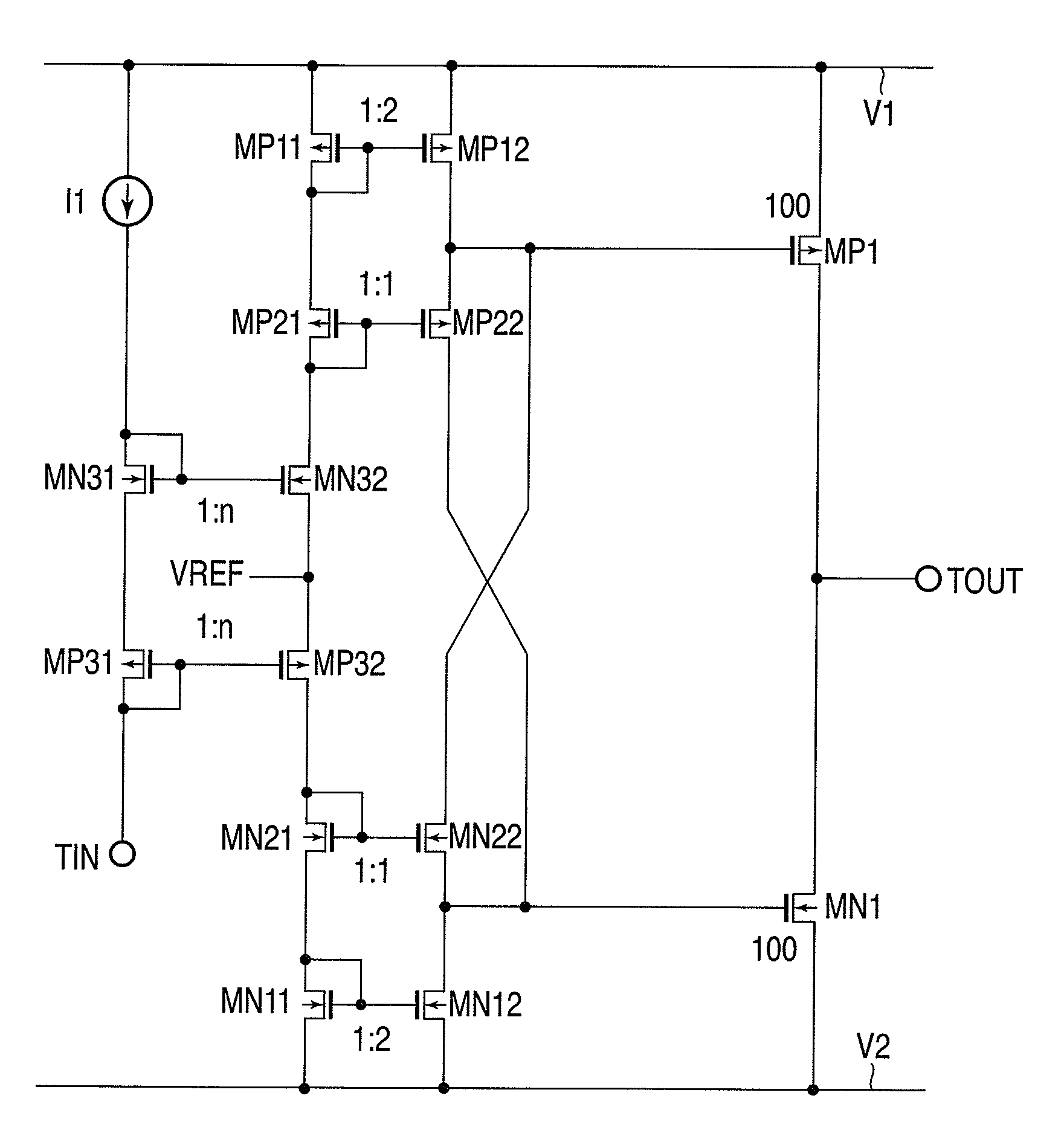
[0033]An output circuit according to the first embodiment is described. FIG. 4 is a circuit diagram showing the detailed configuration of the output circuit according to the first embodiment.

[0034][2-1] Circuit Configuration

[0035]As shown in FIG. 4, a gm amplifier AP1 comprises an input terminal TIN, a reference voltage VREF, n-channel MOS transistors MN31, MN32, p-channel MOS transistors MP31, MP32 and a current source I1.

[0036]A current mirror circuit CMP1 comprises p-channel MOS transistors MP11, MP12. A current mirror circuit CMP2 comprises p-channel MOS transistors MP21, MP22. A current mirror circuit CMN1 comprises n-channel MOS transistors MN11, MN12. A current mirror circuit CMN2 comprises n-channel MOS transistors MN21, MN22.

[0037]A gate of an output transistor MP1 connected between a first power supply rail V1 and an output terminal TOUT is connected between MOS transistors MP12, MP22 and also connected to a drain of MOS transistor MN22. A gate of an ou...

second embodiment

[3] Second Embodiment

[0092]An output circuit according to the second embodiment is described. FIG. 6 is a circuit diagram showing the detailed configuration of the output circuit according to the second embodiment.

[0093][3-1] Circuit Configuration

[0094]In the second embodiment, the MOS transistors configuring the gm amplifier AP1 and the current mirror circuits CMP2, CMN2 in the first embodiment are replaced with bipolar transistors.

[0095]More specifically, as shown in FIG. 6, a gm amplifier AP1 comprises npn bipolar transistors QN31, QN32, pnp bipolar transistors QP31, QP32 and a current source I1. An intermediate voltage VINT is supplied between bipolar transistors QP31, QP32.

[0096]A current mirror CMP2 comprises pnp bipolar transistors QP21, QP22. A current mirror CMN1 comprises npn bipolar transistors QN21, QN22.

[0097]Other components are similar to those in the first embodiment. In addition, output transistors MP1, MN1, MOS transistors MP11, MP12 configuring the current mirror ...

third embodiment

[4] Third Embodiment

[0099]An output circuit according to the third embodiment is described. FIG. 7 is a circuit diagram showing the detailed configuration of the output circuit according to the third embodiment.

[0100][4-1] Circuit Configuration

[0101]The third embodiment is different from the first embodiment in that a connection point between MOS transistors MN31, MP31 is an input terminal. Moreover, an intermediate voltage VINT is supplied between MOS transistors MN32, MP32.

[0102]As shown in FIG. 7, a gm amplifier AP1 comprises the MOS transistors MN31, MN32, MP31, MP32 and two current sources I1.

[0103]Circuit operation and advantages in the output circuit according to the third embodiment are similar to those in the first embodiment and are not described.


PUM


Abstract

According to one embodiment, a first transistor is connected between a first power supply rail and an output unit. A second transistor is connected between the output unit and a second power supply rail. A gm amplifier includes an input unit and first and second output terminals and amplifies a difference between a signal input to the input unit and a reference voltage. First and second current mirror circuits are connected to be vertically stacked between the first rail and the first terminal as well as a gate of the second transistor. Third and fourth current mirror circuits are connected to be vertically stacked between the second rail and the second terminal as well as a gate of the first transistor. The gate of the first transistor is connected to the first and second circuits. The gate of the second transistor is connected to the third and fourth circuits.

Description

CROSS-REFERENCE TO RELATED APPLICATIONS[0001]This application is based upon and claims the benefit of priority from Japanese Patent Application No. 2010-000745, filed Jan. 5, 2010; the entire contents of which are incorporated herein by reference.FIELD[0002]Embodiments described herein relate generally to a push-pull output circuit. The push-pull output circuit is used, for example, in a power amplifier circuit.BACKGROUND[0003]One example of a conventional MOS output circuit is described in, for example, the specification of Japanese Patent No. 4030277. According to this MOS output circuit, a change in the gate impedance of an output transistor in a no-signal condition and during signal input can be reduced by a simple configuration. Thus, a low-strain analog MOS amplifier circuit can be obtained without any increase in chip size.[0004]However, because of the action of a circuit which comprises, for example, a MOS transistor and a resistance and which is configured to determine an i...

Claims


Application Information

Patent Timeline
IPC IPC(8): H03F3/18
CPCH03F3/3045H03F3/305H03F3/45183H03F2203/45674
Inventor TSURUMI, HIROYUKI
Owner KK TOSHIBA
Why Eureka
Try Eureka