Optical image modulator, optical apparatus including the same, and methods of manufacturing and operating the optical image modulator

a technology of optical image and optical apparatus, applied in the direction of optics, semiconductor devices, instruments, etc., can solve the problems of noise, emitted light is unnecessary, and part of light scattered in the light emitting device is absorbed by the light receiving device, so as to prevent optical interference and efficiently use incident light

Active Publication Date: 2012-06-05
SAMSUNG ELECTRONICS CO LTD +1
View PDF18 Cites 7 Cited by
  • Summary
  • Abstract
  • Description
  • Claims
  • Application Information

AI Technical Summary

Benefits of technology

[0009]One or more exemplary embodiments of the present invention include an optical image modulator that may prevent optical interference between a light receiving device and a light emitting device and efficiently use incident light.
[0025]According to one or more exemplary embodiments of the present invention, there is provided a method of manufacturing an optical image modulator having an optical-electric device and an electric-optical device which are sequentially disposed, the method including forming a first light amount increasing unit between the electric-optical device and the optical-electric device, wherein the first light amount increasing unit increases the amount of forward light emission of the electric-optical device.

Problems solved by technology

Since a light receiving device and a light emitting device in such an OEO image modulator are close to each other, the risk of optical interference between the light receiving device and the light emitting device is very high.
However, part of light scattered in the light emitting device is absorbed by the light receiving device.
The emitted light is unnecessary and becomes noise, thereby acting as a noise component to a normal image output from the OEO image modulator.
The noise component may degrade the quality and reliability of the normal image, and degrade the modulation efficiency of the OEO image modulator as well.

Method used


Image

  • Optical image modulator, optical apparatus including the same, and methods of manufacturing and operating the optical image modulator
  • Optical image modulator, optical apparatus including the same, and methods of manufacturing and operating the optical image modulator
  • Optical image modulator, optical apparatus including the same, and methods of manufacturing and operating the optical image modulator

Examples


Embodiment Construction

[0046]Reference will now be made in detail to the exemplary embodiments, examples of which are illustrated in the accompanying drawings. The thicknesses of layers or regions illustrated in the drawings are exaggerated for clarity.

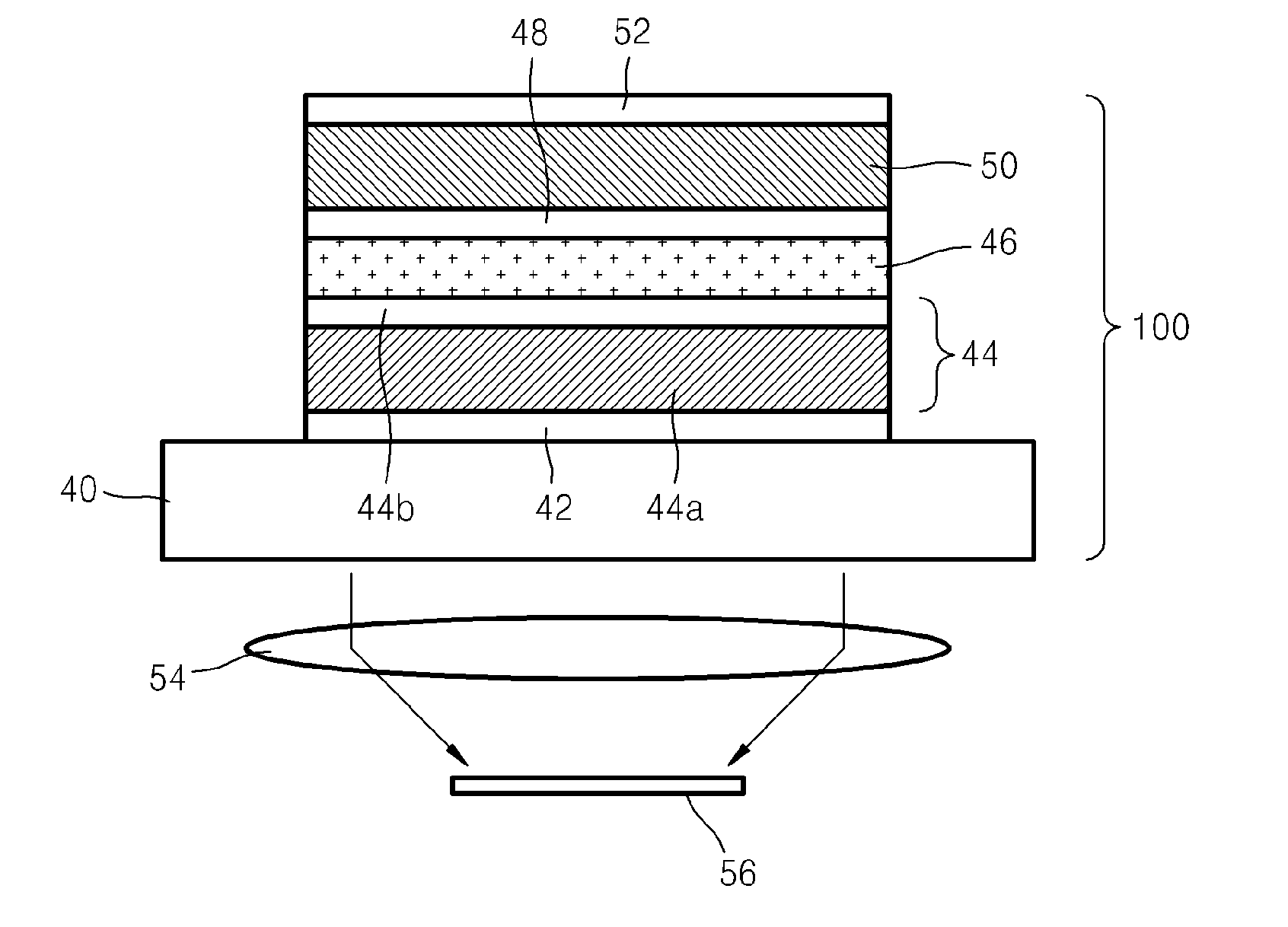
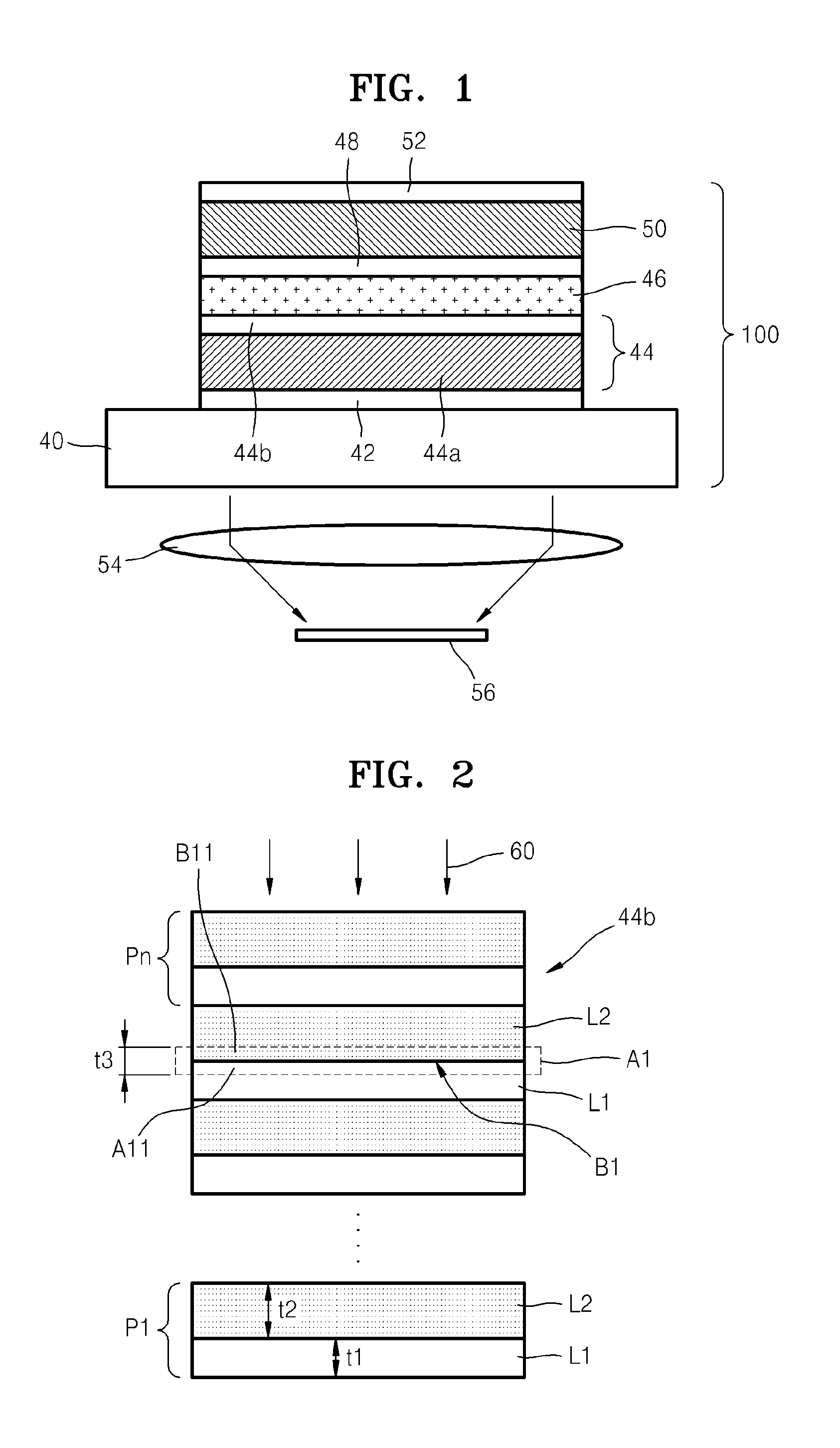
[0047]FIG. 1 is a cross-sectional view of an optical image modulator 100 according to an embodiment of the present invention.

[0048]Referring to FIG. 1, the optical image modulator 100 may include a transparent substrate 40, a first transparent electrode layer 42, an electric-optical unit 44, an interface layer 46, an internal semiconductor electrode layer 48, an optical-electric device 50, and a second transparent electrode layer 52. Although the first transparent electrode layer 42, the electric-optical unit 44, the interface layer 46, the internal semiconductor electrode layer 48, the optical-electric device 50, and the second transparent electrode layer 52 are stacked sequentially on the transparent substrate 40 in FIG. 1, the elements may be stacked in ...


PUM

PropertyMeasurementUnit
near infrared (NIR)-IR wavelengthsaaaaaaaaaa
wavelengthsaaaaaaaaaa
central wavelengthaaaaaaaaaa

Abstract

Disclosed are an optical image modulator, an optical apparatus including the same, and methods of manufacturing and operating the optical image modulator. The optical image modulator includes a light amount increasing unit increasing the amount of forward light emission of an electric-optical unit. The light amount increasing unit includes a first reflector reflecting light, which travels from the inside of the electric-optical unit toward the optical-electric unit, to the electric-optical unit. The light amount increasing unit may further include a second light reflector reflecting light, which passes through the optical-electric unit without optical-electric conversion, to the optical-electric unit.

Description

CROSS-REFERENCE TO RELATED APPLICATIONS[0001]This application claims the benefit of Korean Patent Application No. 10-2009-0003405, filed on Jan. 15, 2009, in the Korean Intellectual Property Office, the disclosure of which is incorporated herein in its entirety by reference.BACKGROUND[0002]1. Field[0003]One or more exemplary embodiments of the present invention relate to an optical image modulator, an optical apparatus including the same, and methods of manufacturing and operating the optical image modulator.[0004]2. Description of the Related Art[0005]Optical image modulators are used in imaging systems such as a laser radar (LADAR) and an infrared (IR) camera. Optical image modulators receive optical information about an object, modulate the brightness of the optical information to vary wavelengths, and transmit the modulated optical information to an optical image sensor such as a charge-coupled device (CCD).[0006]In particular, optical-electric-optical (OEO) image modulators ref...

Claims


Application Information

Patent Timeline
Patent Type & Authority Patents(United States)
IPC IPC(8): G02F1/03G02B1/10
CPCG02B27/0006G02B13/008G02B1/10H01L27/14H04N25/00G02B26/0816
Inventor PARK, YONG-HWAJANG, JAE-HYUNGCHO, YONG-CHULPARK, CHANG-SOOLEE, BYEONG-HA
Owner SAMSUNG ELECTRONICS CO LTD
Why Eureka
Try Eureka