Die singulation method and package formed thereby

a technology of singulation and die, which is applied in the field of semiconductor/solid-state device manufacturing, electrical equipment, basic electric elements, etc., can solve the problems of limiting the number of devices which can be fabricated from semiconductor wafers, contaminating devices, and affecting the shape of devices,

Active Publication Date: 2012-08-07
NAT TECH & ENG SOLUTIONS OF SANDIA LLC
View PDF7 Cites 18 Cited by
  • Summary
  • Abstract
  • Description
  • Claims
  • Application Information

AI Technical Summary

Benefits of technology

[0022]In some embodiments of the present invention, the die can include one or more stops thereon, with each stop being

Problems solved by technology

The use of saw cutting requires a spacing (i.e. a street) between adjacent devices which are being singulated with this spacing being up to 100 microns or more wide; and this spacing limits the number of devices which can be fabricated from the semiconductor wafer.
Additionally, saw cutting generates debris which can contaminate the devices or become lodged in moveable members of MEMS devices or in fluid channels of microfluidic devices.
Furthermore, saw cutting must be performed along straight

Method used


Image

  • Die singulation method and package formed thereby
  • Die singulation method and package formed thereby
  • Die singulation method and package formed thereby

Examples


Embodiment Construction

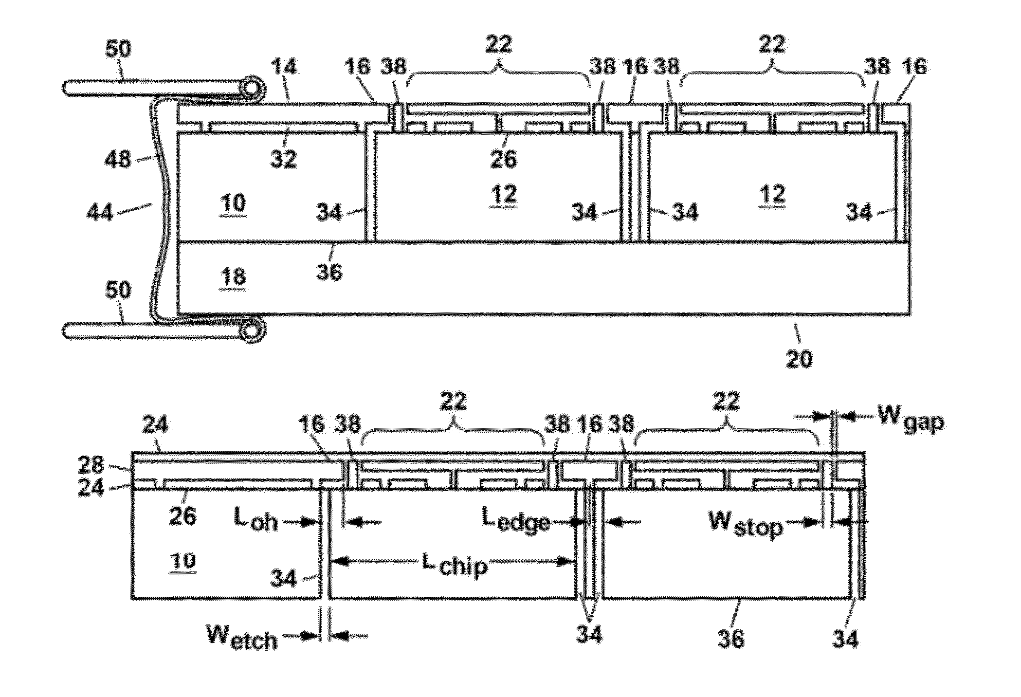
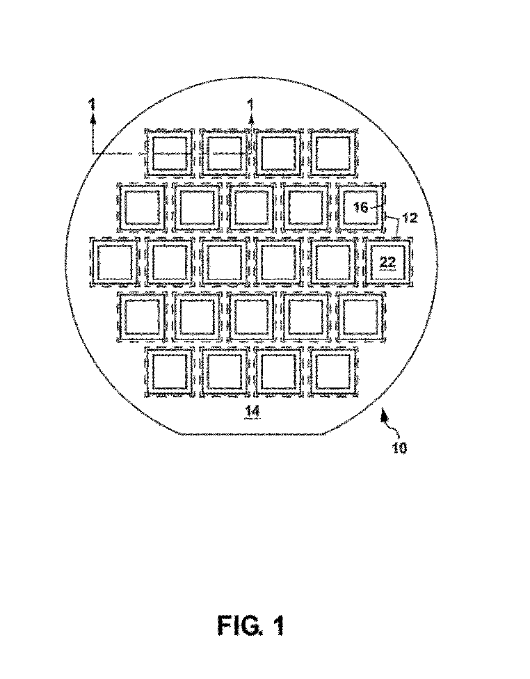
[0032]FIG. 1 shows a schematic plan view of a substrate 10 which can be processed according to the method 100 of the present invention illustrated in FIG. 2 to form one or more singulated die 12. The substrate 10 can comprise a semiconductor substrate although those skilled in the art will understand that the method of the present invention can also be applied to other types of substrates including metal substrates, polymer substrates, and substrates formed of insulating dielectric materials (e.g. alumina, fused silica, crystalline quartz, etc.). In FIG. 1, each singulated die 12 is indicated by a dashed box. The method 100 also forms a frame 14 about the singulated die 12 from a portion of the substrate 10 which is not used for the die 12, with the frame having a retainer 16 which extends over the singulated die 12 to hold the die 12 in place after singulation. The frame 14 together with a handle wafer 18 located beneath the frame 14 can also form a package 20 for holding, transpor...


PUM


Abstract

A method is disclosed for singulating die from a substrate having a sacrificial layer and one or more device layers, with a retainer being formed in the device layer(s) and anchored to the substrate. Deep Reactive Ion Etching (DRIE) etching of a trench through the substrate from the bottom side defines a shape for each die. A handle wafer is then attached to the bottom side of the substrate, and the sacrificial layer is etched to singulate the die and to form a frame from the retainer and the substrate. The frame and handle wafer, which retain the singulated die in place, can be attached together with a clamp or a clip and to form a package for the singulated die. One or more stops can be formed from the device layer(s) to limit a sliding motion of the singulated die.

Description

GOVERNMENT RIGHTS[0001]This invention was made with Government support under Contract No. DE-AC 04-94AL85000 awarded by the U.S. Department of Energy. The Government has certain rights in the invention.CROSS REFERENCE TO RELATED APPLICATIONS[0002]The present application is related to U.S. patent application Ser. No. 12 / 758,838, entitled “Die Singulation Method” of common assignee which is being filed on the same date as this application, the contents of which are incorporated herein by reference in their entirety.FIELD OF THE INVENTION[0003]The present invention relates in general to semiconductor processing, and in particular to a method for singulating one or more die from a substrate by etching and to a package for the singulated die which is formed upon singulation of the die using the method of the present invention.BACKGROUND OF THE INVENTION[0004]A large number of semiconductor devices are typically fabricated on a common semiconductor wafer having a diameter up to 12 inches ...

Claims


Application Information

Patent Timeline
IPC IPC(8): H01L21/00
CPCH01L21/78
Inventor ANDERSON, ROBERT C.SHUL, RANDY J.CLEWS, PEGGY J.BAKER, MICHAEL S.DE BOER, MAARTEN P.
Owner NAT TECH & ENG SOLUTIONS OF SANDIA LLC
Why Eureka
Try Eureka