Chemical-mechanical planarization method and method for fabricating metal gate in gate-last process

a technology of metal gate and gate-last, which is applied in the direction of basic electric elements, electrical equipment, and semiconductor devices, can solve the problems of short circuit in the device, limit the tuning range of metal gate cmp process, etc., and achieve the effect of improving the uniformity of the inner die and preventing short circuits in the devi

Active Publication Date: 2012-08-28
INST OF MICROELECTRONICS CHINESE ACAD OF SCI
View PDF8 Cites 9 Cited by
  • Summary
  • Abstract
  • Description
  • Claims
  • Application Information

AI Technical Summary

Benefits of technology

[0007]A problem to be solved by the present invention is to provide a chemical-mechanical planarization method, with improved within-die uniformity and thereby preventing short circuits in the device.
[0030]Compared with the prior art, the technical solution above has the following advantages.
[0031]Selectively doping is performed on the insulating layer, and only the protruding part of the insulting layer is doped, destroying the chemical bonds and crystal structures in the protruding part of the insulting layer. Hence, the corrosive attacks on the material of the protruding part by the slurry in the CMP are enhanced, and the removal rate of the material of the protruding part by the CMP is greatly increased, thereby improving the within-die uniformity of the process, avoiding the thickness variation of the insulating layer being passed down the planarized substrate surface, and reducing or even eliminating the dishing on the insulating layer between gates.
[0032]Consequently, in the subsequent process of metal-gate formation, there will not be metal residue in the insulating layer between gates, thereby preventing short circuits in the device.

Problems solved by technology

The gate-last approach presents a challenge in developing the chemical and mechanical planarization (CMP) process.
As shown in FIG. 3 and FIG. 4, the dishing 14 on the silicon dioxide insulating layer will be filled with metal in a subsequent metal-gate deposition process, drastically limiting the tuning range of metal-gate CMP process, resulting in metal residue between gates and causing a short circuit in the device.

Method used


Image

  • Chemical-mechanical planarization method and method for fabricating metal gate in gate-last process
  • Chemical-mechanical planarization method and method for fabricating metal gate in gate-last process
  • Chemical-mechanical planarization method and method for fabricating metal gate in gate-last process

Examples


embodiment 1

[0044]FIG. 5 illustrates a flow chart of a CMP method according to the embodiment; and FIG. 6—FIG. 8 illustrate the CMP method according to the embodiment.

[0045]As shown in the figures, the method includes:

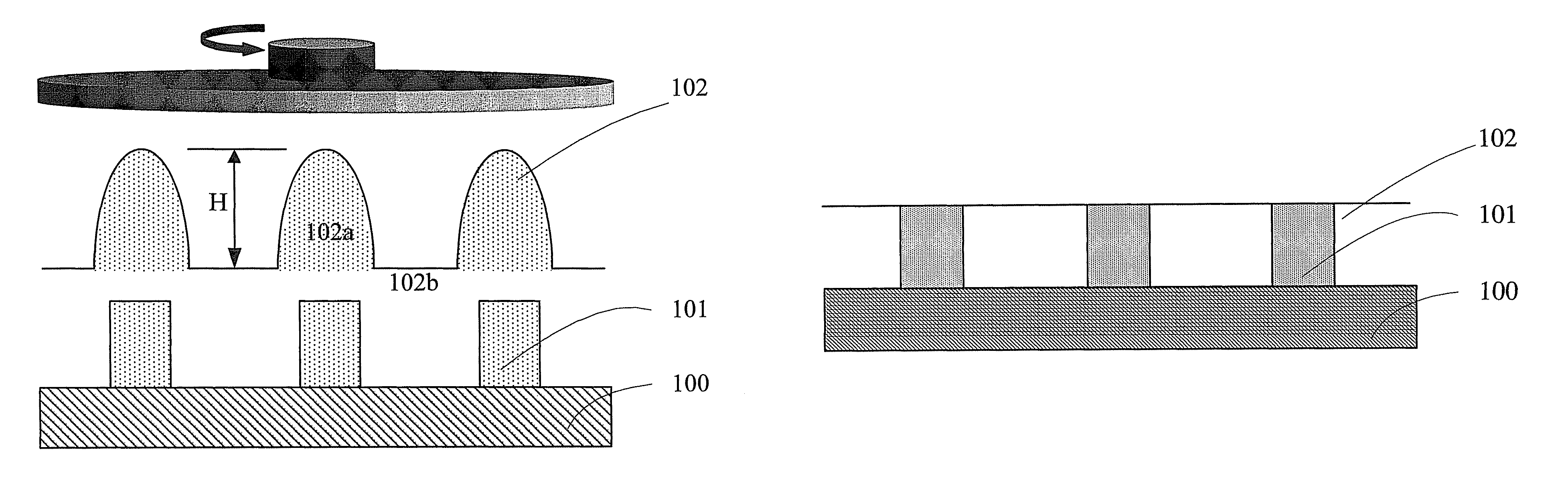
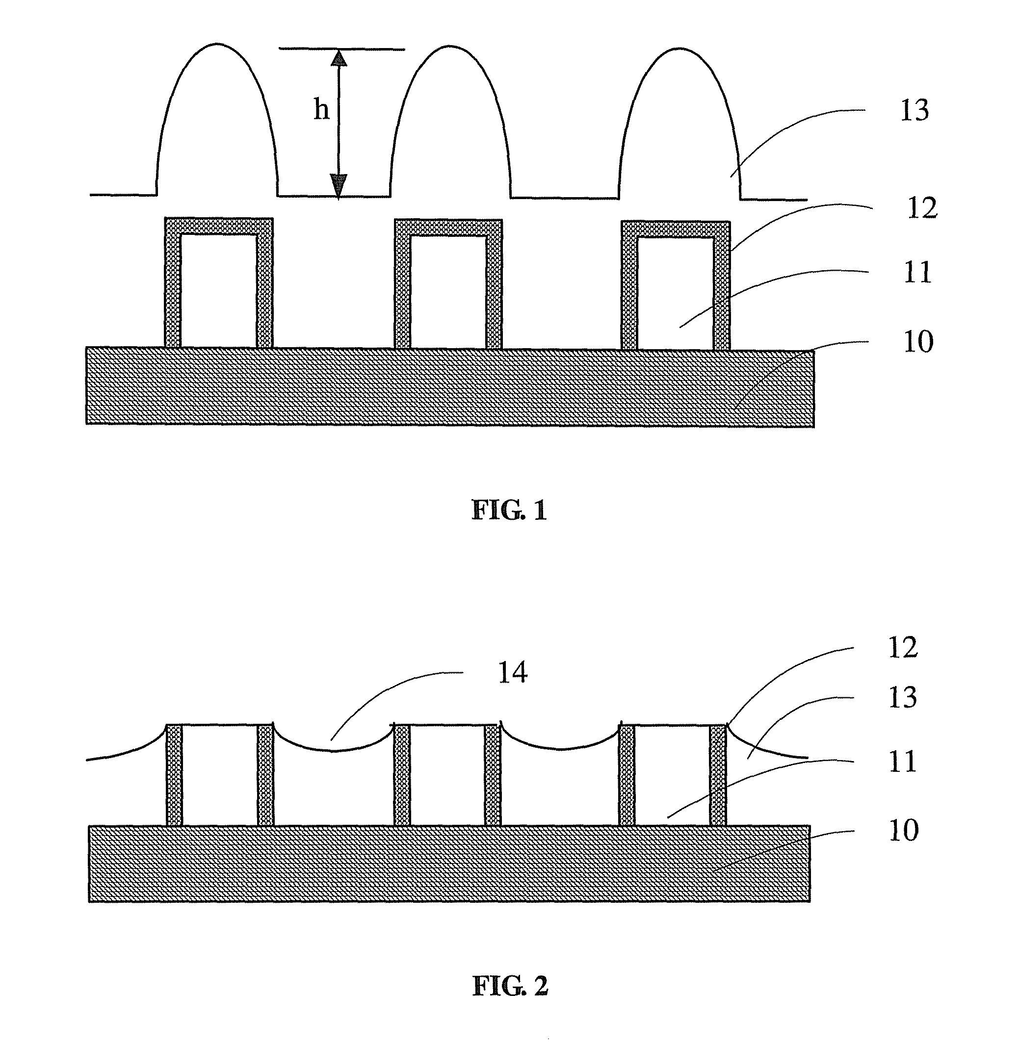
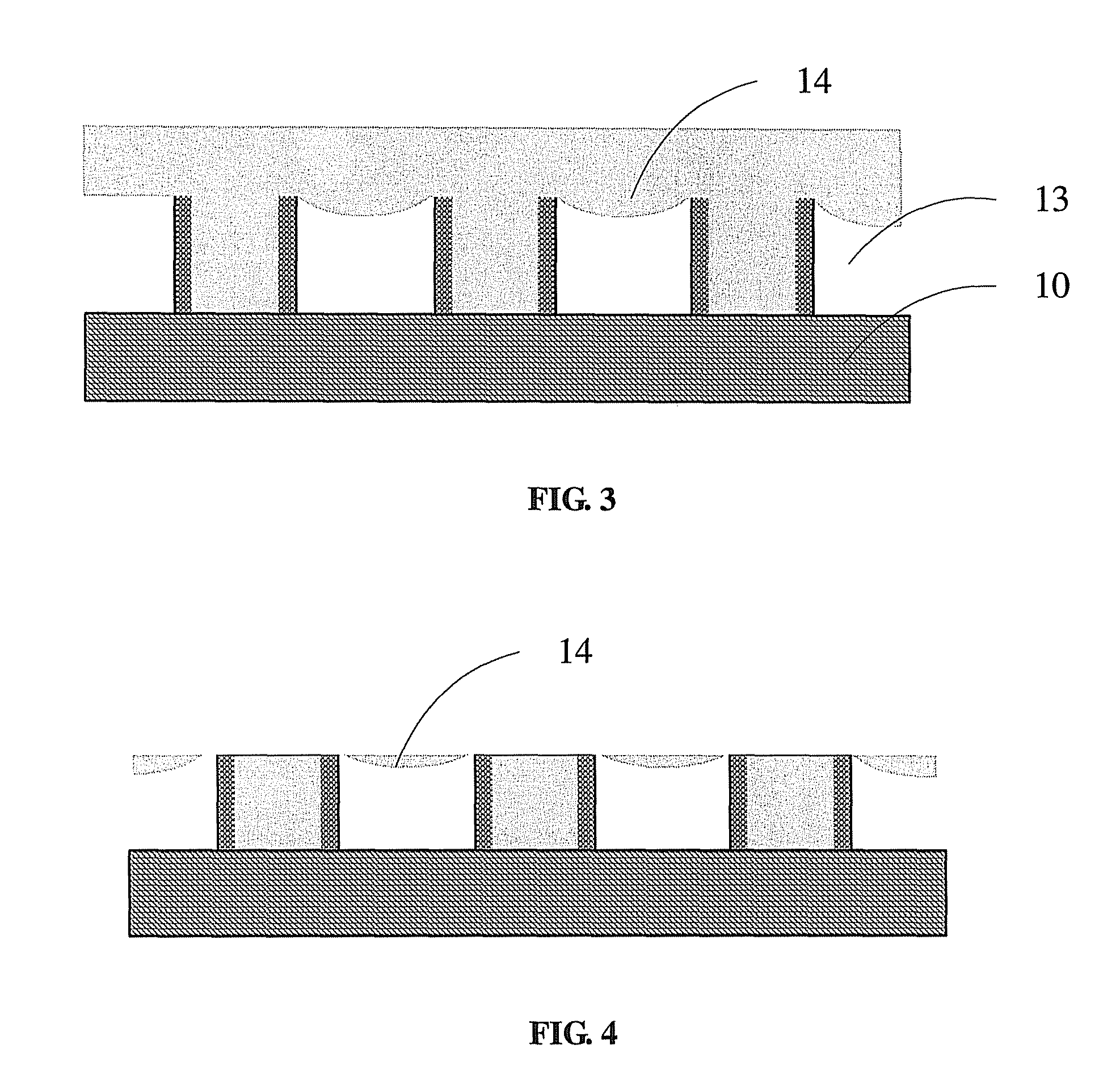
[0046]Step S1: as shown in FIG. 6, a substrate 100 is provided, including a gate 101 and source / drain regions (not shown) on the sides of the gate 101, the gate 101 and the source / drain regions are overlay by an insulating layer 102, and the insulating layer 102 includes a protruding part 102a above the gate and a recessed part 102b above the surface of the substrate between the gates 101.

[0047]Step S2: selective doping is performed on the insulating layer 102, such that only the protruding part 102a is doped. Preferably, in this embodiment, the selective doping is ion implantation; and a mask layer 103 covers the recessed part 102b of the insulating layer 102, with only the protruding part 102a exposed, and the protruding part 102a is doped through ion implantation in the directi...

embodiment 2

[0054]As an example, a gate-last method for fabricating a typical 32 nm metal gate is described, to show another embodiment of the CMP method. FIG. 9—FIG. 16 illustrate a method for fabricating a metal gate in gate last process according to the embodiment.

[0055]As shown in FIG. 9, a substrate 200 is provided, the substrate 200 includes a dummy gate 201, a gate oxide layer (not shown) and source / drain regions (not shown) on the sides of the dummy gate 200, and the dummy gate 201 and the source / drain regions are overlay by a first insulating layer 208 and a second insulating layer 202.

[0056]Specifically, the substrate 200 may be formed of an elemental semiconductor, e.g., monocrystalline, polycrystalline or amorphous silicon, or monocrystalline, polycrystalline or amorphous silicon-germanium (SiGe); or a compound semiconductor, e.g., silicon carbide (SiC), indium antimonide (InSb), lead telluride (PbTe), indium arsenide (InAs), indium phosphide (InP), gallium arsenide (GaAs), or galli...


PUM


Abstract

The present invention provides a chemical-mechanical planarization method. The chemical-mechanical planarization method includes: providing a substrate including a gate and source / drain regions on the sides of the gate, the gate and the source / drain regions being overlay by an insulating layer, and the insulating layer including a protruding part above the gate and a recessed part above a surface of the substrate between gates; selectively doping the insulating layer such that only the protruding part is doped; and performing CMP on the substrate after doping, to remove the protruding part and planarize the surface of the substrate. By selectively doping the insulating layer, the method makes only the protruding part of the insulating layer doped, enhancing the corrosive attacks on the material of the protruding part by the slurry in the CMP, and increasing the removal rate of the material of the protruding part by the CMP.

Description

CROSS-REFERENCE TO RELATED APPLICATION[0001]This application is a Section 371 national stage application of International Application No. PCT / CN2011 / 072643 filed on Apr. 12, 2011, which claims priority to CN201010567260.9 filed on Nov. 30, 2010, the contents of which are incorporated herein by reference in their entirety.FIELD OF THE INVENTION[0002]The present invention relates to the field of integrated circuit technology, and in particular to a chemical-mechanical planarization method.BACKGROUND OF THE INVENTION[0003]Driven by increasing demands for ultra-large-scale integration and high performance of integrated circuits, semiconductor technology has been scaled down the 45 nm and even smaller technology node. The success of high-k metal-gate (HKMG) in the 45 nm technology node has made it key to the process flow for the sub-30 nm technology node. Intel, who has committed to a metal-gate-last approach, is the leader and only one manufacturer in mass production of 45 nm and 32 nm ...

Claims


Application Information

Patent Timeline
Patent Type & Authority Patents(United States)
IPC IPC(8): H01L21/302
CPCH01L21/31053H01L21/31155H01L29/66545H01L29/66606H01L29/78
Inventor YANG, TAOLIU, JINBIAOHE, XIAOBINZHAO, CHAOCHEN, DAPENG
Owner INST OF MICROELECTRONICS CHINESE ACAD OF SCI
Why Eureka
Try Eureka