Semiconductor device comprising self-aligned contact elements

a contact element and silicon dioxide technology, applied in the direction of semiconductor devices, electrical devices, transistors, etc., can solve the problems of severe device failure, silicon dioxide-based gate dielectric may no longer be compatible with thermal design power requirements, and the limiting factor of the finally achieved operating speed of complex integrated circuits is no longer, so as to avoid extremely critical lithography processes, avoid short circuits, and avoid short circuits.

Active Publication Date: 2012-08-23
GLOBALFOUNDRIES US INC
View PDF12 Cites 45 Cited by
  • Summary
  • Abstract
  • Description
  • Claims
  • Application Information

AI Technical Summary

Benefits of technology

[0018]Generally, the present disclosure provides semiconductor devices and manufacturing techniques in which replacement gate approaches may be applied so as to form high-k metal gate electrode structures, for instance as required for sophisticated transistor elements in logic circuit portions and the like, while at the same time contact elements connecting to the active region of the transistors may be provided in a self-aligned manner. That is, the contact elements may be provided so as to be self-aligned with respect to the gate electrode structures in a length direction, thereby avoiding extremely critical lithography processes that may be required in conventional strategies in order to appropriately position the contact elements in the length direction of the transistors. In order to achieve high compatibility with the replacement gate approach, the contact elements may be formed prior to replacing the placeholder material of the gate electrode structures so that the gate electrode structures are still appropriately encapsulated when forming the contact elements. To this end, in some illustrative embodiments disclosed herein, a less critical lithography process may be applied in the presence of a portion of the interlayer dielectric material by using an appropriate etch mask, which may substantially define the shape and size of the resulting contact elements in the transistor width direction, wherein, in some illustrative embodiments, the size of the corresponding mask opening may be comparable to the size of the active region, while nevertheless ensuring a sufficient process margin with respect to tip portions of the gate electrode structures in order to avoid short circuits between the drain region and the source region. Furthermore, by appropriately defining “exclusion zones” within the active region, i.e., zones in which the self-aligned contact elements connecting to the active region are not provided, even a contacting of gate electrode structures partially or completely within the lateral dimensions of the active region may be realized, thereby significantly reducing the required lateral area for a given circuit configuration. That is, at least some of the gate-to-gate connections may be routed partially above the active region, contrary to conventional design strategies in which generally the gate electrode structures are contacted over isolation regions.
[0019]In other illustrative embodiments, the contact material may be provided in an early manufacturing stage, i.e., prior to actually forming the interlayer dielectric material, thereby also providing the contact material in a “self-aligned” manner, with a subsequent patterning thereof, and may be accomplished on the basis of substantially planar surface topography, wherein less critical lithography conditions are obtained since the actual patterning may be required along the transistor width direction only. Therefore, during this patterning process, the corresponding “opening” formed so as to separate the contact elements with respect to the transistor width direction may be controlled by additional deposition processes, if required, thereby even further enhancing the “resolution” of the resulting patterning process. Subsequently, the opening may be filled with an appropriate dielectric material, wherein the formation of any voids is not critical, thereby providing superior flexibility in selecting appropriate interlayer dielectric materials and deposition techniques.

Problems solved by technology

Due to the reduced dimensions, the operating speed of the circuit components has been increased with every new device generation, wherein, however, the limiting factor of the finally achieved operating speed of complex integrated circuits is no longer the individual transistor element but the electrical performance of the complex wiring system, which may be formed above the device level including the actual semiconductor-based circuit elements, such as transistors and the like.
In this case, however, the resulting leakage currents caused by hard carrier injection direct tunneling of charge carriers through the extremely thin silicon dioxide-based gate dielectric may no longer be compatible with thermal design power requirements.
In this case, a severe device failure may occur.
To this end, a plurality of appropriately shaped contact openings are typically formed, thereby requiring extremely sophisticated lithography techniques, which have to ensure a high alignment accuracy, which, however, due to the reduced pitch, may nevertheless result in a certain degree of misalignment as, for instance, shown for the contact elements 125.
In this case, the gate electrode structures have to be reliably encapsulated by any appropriate etch stop material which, however, is not compatible with sophisticated replacement gate approaches, as described above, since here the top surface of the electrode material is exposed and would require a dedicated etch stop material, which in turn would have to be provided on the basis of an extremely complex lithography and patterning process, thereby resulting in even more process non-uniformities.

Method used


Image

  • Semiconductor device comprising self-aligned contact elements
  • Semiconductor device comprising self-aligned contact elements
  • Semiconductor device comprising self-aligned contact elements

Examples


Embodiment Construction

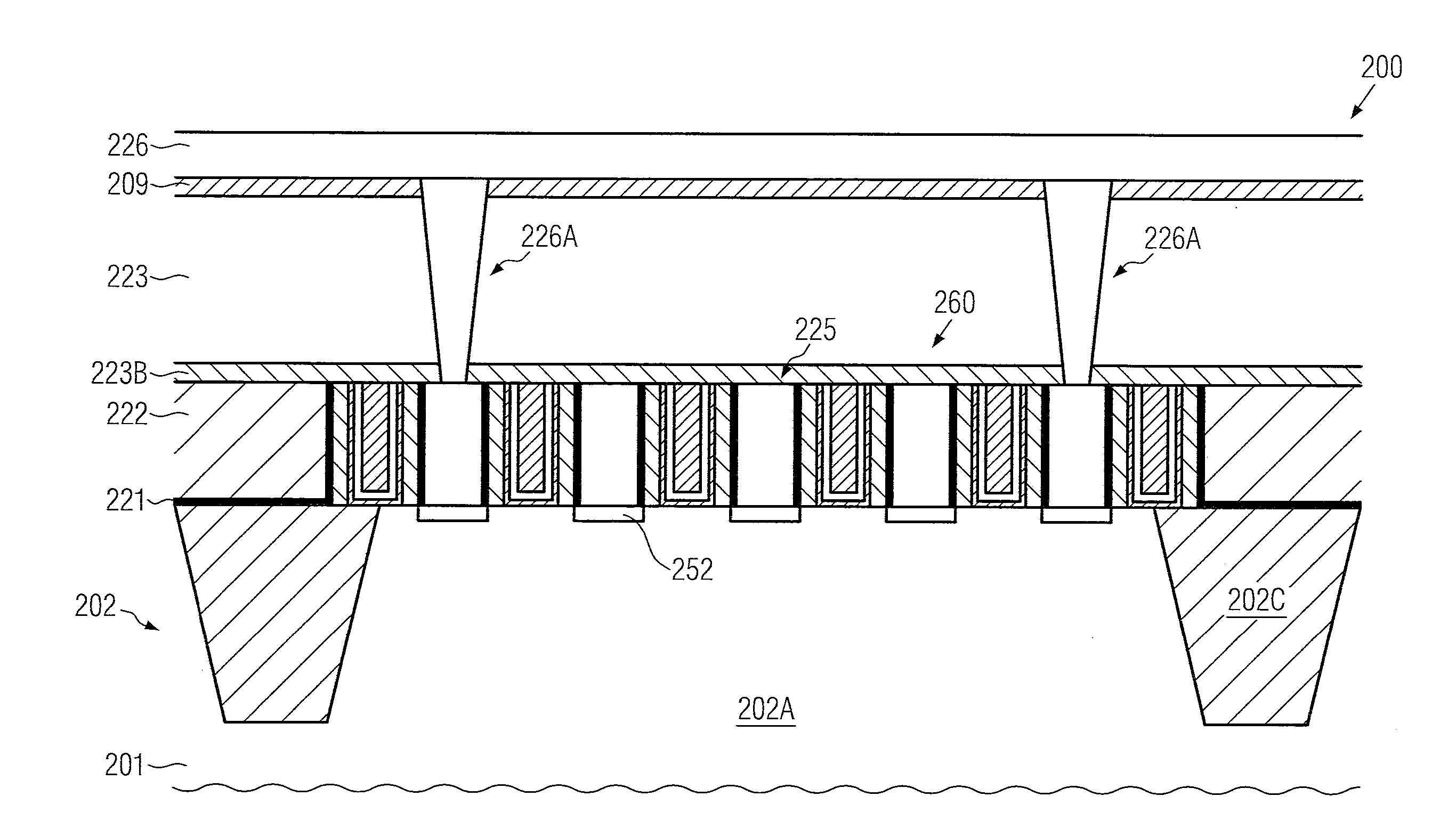
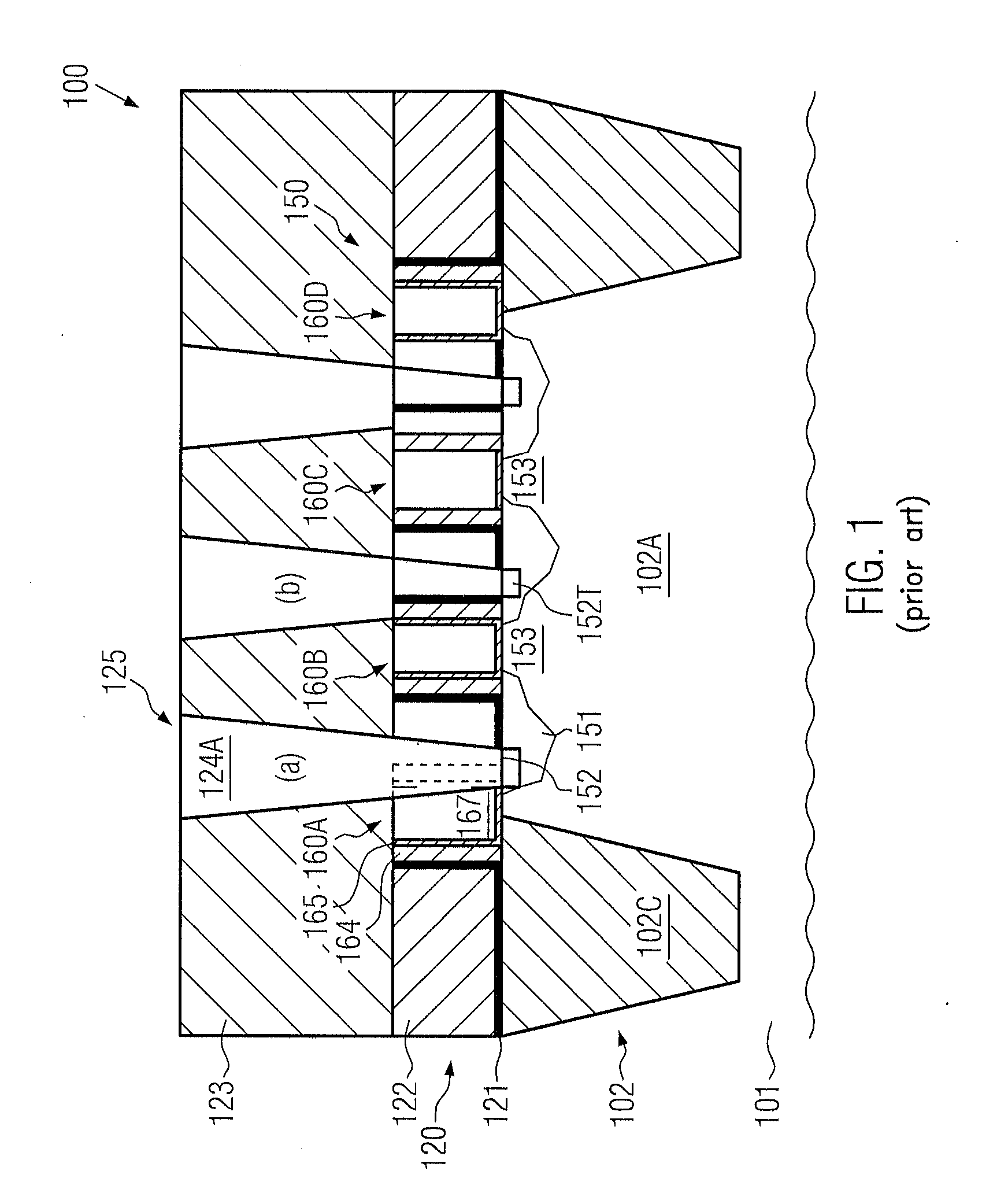
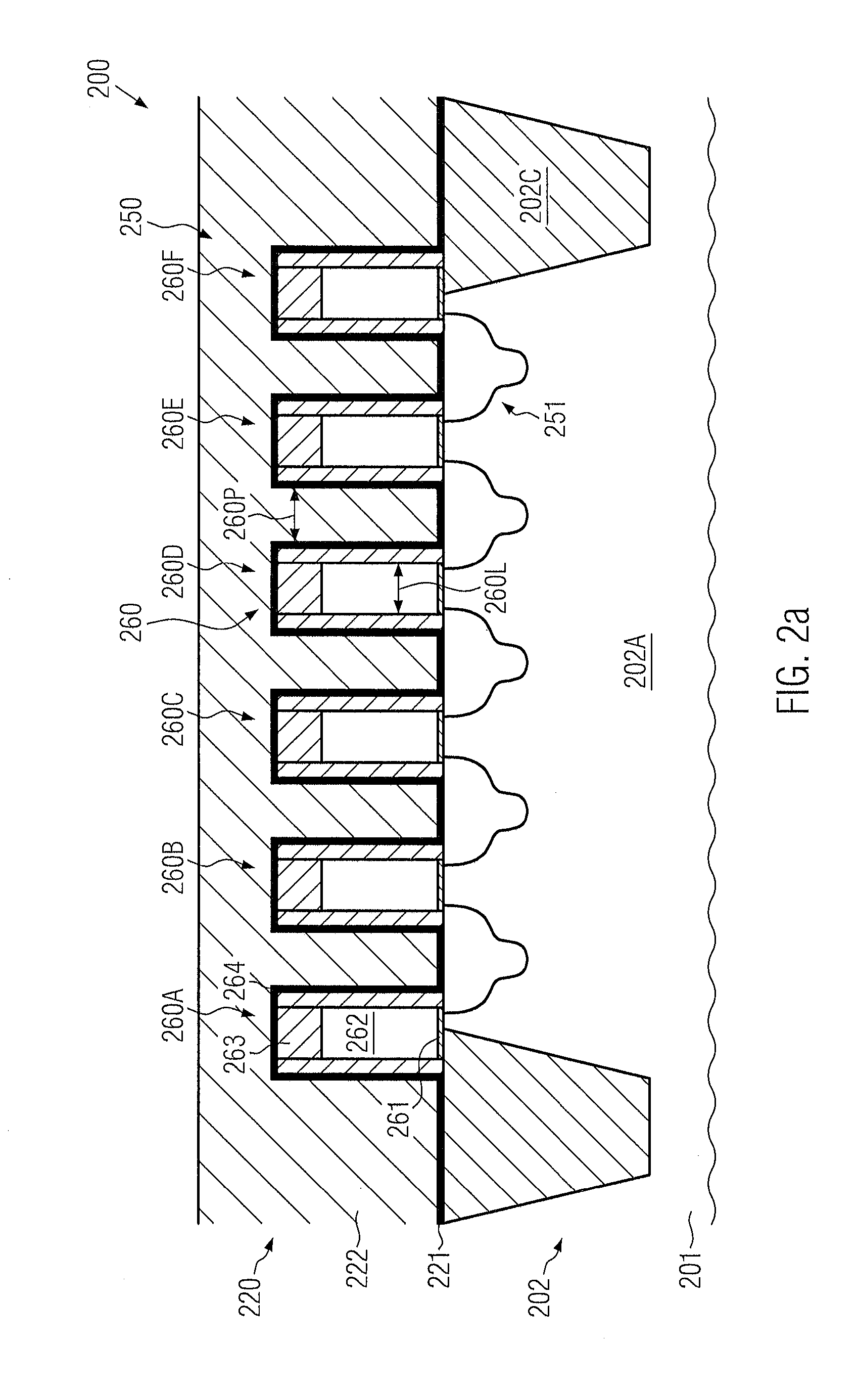
[0036]Various illustrative embodiments of the invention are described below. In the interest of clarity, not all features of an actual implementation are described in this specification. It will of course be appreciated that in the development of any such actual embodiment, numerous implementation-specific decisions must be made to achieve the developers' specific goals, such as compliance with system-related and business-related constraints, which will vary from one implementation to another. Moreover, it will be appreciated that such a development effort might be complex and time-consuming, but would nevertheless be a routine undertaking for those of ordinary skill in the art having the benefit of this disclosure.

[0037]The present subject matter will now be described with reference to the attached figures. Various structures, systems and devices are schematically depicted in the drawings for purposes of explanation only and so as to not obscure the present disclosure with details ...


PUM


Abstract

When forming sophisticated semiconductor devices, a replacement gate approach may be applied in combination with a self-aligned contact regime by forming the self-aligned contacts prior to replacing the placeholder material of the gate electrode structures.

Description

BACKGROUND OF THE INVENTION[0001]1. Field of the Invention[0002]The present disclosure generally relates to the fabrication of integrated circuits, and, more particularly, to the contact level of a semiconductor device, in which contact areas, such as drain and source regions, as well as gate electrode structures, are connected to the metallization system of the semiconductor device.[0003]2. Description of the Related Art[0004]In modern integrated circuits, such as microprocessors, storage devices and the like, a very high number of circuit elements, especially transistors, are provided and operated on a restricted chip area. Although immense progress has been made over recent decades with respect to increased performance and reduced feature sizes of the circuit elements, the ongoing demand for enhanced functionality of electronic devices forces semiconductor manufacturers to steadily reduce the dimensions of the circuit elements and to increase the operating speed thereof. The cont...

Claims


Application Information

Patent Timeline
Patent Type & Authority Applications(United States)
IPC IPC(8): H01L21/28H01L21/283H01L27/088
CPCH01L21/823437H01L21/823475H01L29/66636H01L21/76816H01L21/76895H01L21/76897H01L21/28518H01L29/7848
Inventor BAARS, PETERSCHLOESSER, TILLJAKUBOWSKI, FRANKWEI, ANDYCARTER, RICHARDSCHALLER, MATTHIAS
Owner GLOBALFOUNDRIES US INC
Why Eureka
Try Eureka