Film formation method and film formation apparatus
a film formation method and film technology, applied in the direction of coatings, chemical vapor deposition coatings, electric discharge tubes, etc., can solve the problems of difficult removal and inability to remove cu films, and achieve the effect of efficient control of metal film deposits
- Summary
- Abstract
- Description
- Claims
- Application Information
AI Technical Summary
Benefits of technology
Problems solved by technology
Method used
Image

Examples
first embodiment
[First Embodiment]
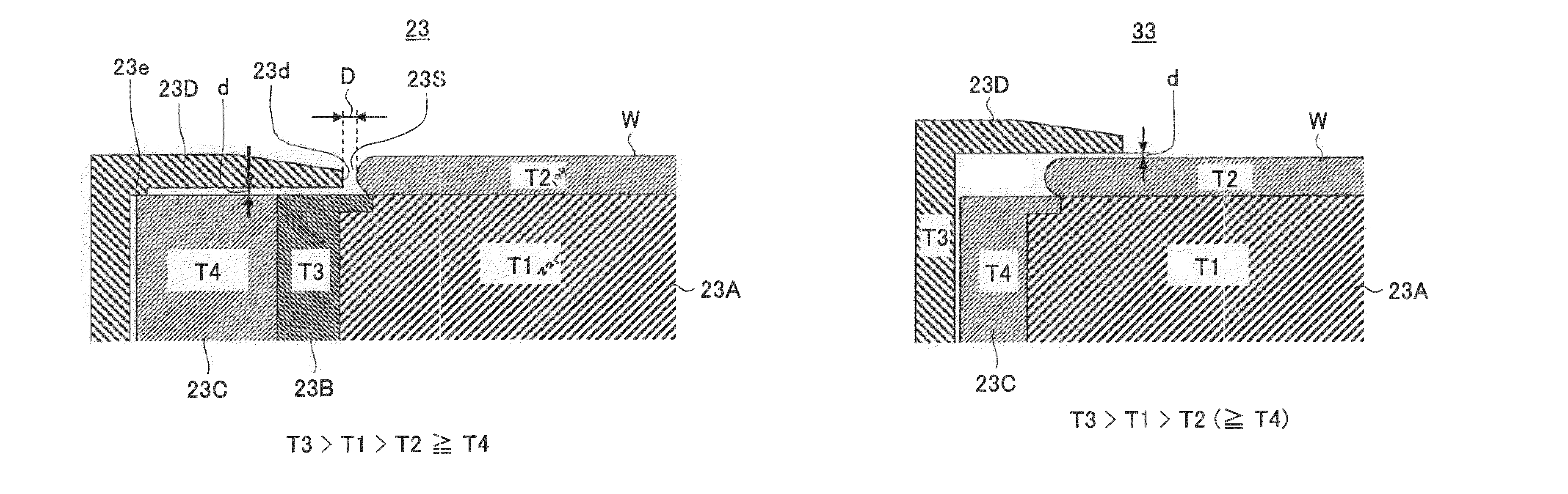
[0046]FIG. 4 schematically shows a configuration of a substrate holder 23 according to a first embodiment of the present invention used in the film formation apparatus 10 in FIG. 1.
[0047]As shown in FIG. 4, the substrate holder 23 includes a supporting section 23A having substantially the same diameter of the wafer “W” to sustain the wafer “W” and a ring-shaped temperature control section 23B outside and in contact with the supporting section 23A. The supporting section 23A is heated to the temperature of “T1” by a first heater (not shown) buried in the supporting section 23A. The temperature control section 23B is heated to the temperature of “T3” which is higher than that of “T1” (T13) by a second heater (not shown).
[0048]Further, outside of the temperature control section 23B, an outer peripheral member 23C is formed so as to constitute an outer peripheral portion of the substrate holder 23. Still further, outside of the outer peripheral member 23C, a cover ring...
second embodiment
[Second Embodiment]
[0055]FIG. 5 schematically shows a configuration of a substrate holder 33 according to a second embodiment of the present invention. In the figure, the same reference numerals are used for the corresponding elements described above and the description of the elements is herein omitted.
[0056]As shown in FIG. 5, in the substrate holder 33, the temperature control section 23B is not included between the supporting section 23A and the outer peripheral member 23C, and the outer peripheral member 23C contiguously covers the outer side of the supporting section 23A.
[0057]Further, in the configuration in FIG. 5, the cover ring 23D is heated to a temperature “T3” which is higher than the temperature “T1” of the supporting section 23A by a heater (not shown) buried in the cover ring 23D.
[0058]The cover ring 23D includes its end portion which covers the peripheral portion of the upper surface of the wafer “W” in a ring shape. As a result, a space is formed having a width of ...
third embodiment
[Third Embodiment]
[0060]FIG. 7 schematically shows a configuration of a substrate holder 43 according to a third embodiment of the present invention. In the figure, the same reference numerals are used for the corresponding elements described above and the description of the elements is herein omitted.
[0061]As shown in FIG. 7, the upper surface of the wafer “W” is held by a clamp ring 23 that is movably provided in up and down directions. The clamp ring 23E is in engaged with the wafer in its lowered position as shown in FIG. 7. When the clamp ring 23E is lifted up to its higher position, the wafer “W” is released.
[0062]When the clamp ring 23E is positioned at its lowered position, the clamp ring 23E is in contact with a heat source 23F that is formed in a ring shape outside the supporting section 23A and that is maintained at the temperature “T5” by a heater RA. As a result, the clamp ring 23E is heated to the temperature “T3” (T35) .
[0063]Further, in the configuration in FIG. 7, t...
PUM
| Property | Measurement | Unit |
|---|---|---|
| diameter | aaaaa | aaaaa |
| diameter | aaaaa | aaaaa |
| distance | aaaaa | aaaaa |
Abstract
Description
Claims
Application Information
 - R&D
- Intellectual Property
- Life Sciences
- Materials
- Tech Scout
- Unparalleled Data Quality
- Higher Quality Content
- 60% Fewer Hallucinations
Browse by: Latest US Patents, China's latest patents, Technical Efficacy Thesaurus, Application Domain, Technology Topic, Popular Technical Reports.
© 2025 PatSnap. All rights reserved.Legal|Privacy policy|Modern Slavery Act Transparency Statement|Sitemap|About US| Contact US: help@patsnap.com