Amplifier system for a power converter

a power converter and amplifier technology, applied in the direction of transistors, solid-state devices, amplifiers with semiconductor devices/discharge tubes, etc., can solve the problems of limiting the voltage and current levels at which the mosfets may reliably operate without destruction, unintended signals (currents) being coupled from high current members to other signal portions of the circuitry, etc., to achieve the effect of reducing the activity of parasitic switching devices

Active Publication Date: 2012-10-09
HARMAN INT IND INC
View PDF4 Cites 5 Cited by
  • Summary
  • Abstract
  • Description
  • Claims
  • Application Information

AI Technical Summary

Benefits of technology

[0006]An amplifier system minimizes activity of parasitic switching devices by reverse biasing at least one parasitic switching device appearing in a substrate of a semiconductor included in the amplifier system. The amplifier system includes switching devices formed in an integrated circuit in a substrate of the semiconductor as power switches, such as power MOSFETS. The switching devices may include a first switching device and a second switching device that are cooperatively switchable in a half bridge power stage configuration to generate an amplified output signal on an output node of the semiconductor. The semiconductor may also include a power supply input node for receiving a power supply voltage and a substrate node coupled with the substrate.
[0011]Yet another interesting feature of the amplifier system is that the system can provide an inexpensive extension of a region of safe operation of the switching devices by keeping the parasitic switching devices substantially turned off. Extension of the region of safe operation of the switching devices can increase power output of the semiconductor. When the parasitic switching devices are kept off, not only are the regions of safe operation of the switching devices extended in terms of higher voltage and current, but also noise currents and electromagnetic interference (EMI) may be reduced. Noise current may result from extended free-wheeling body diode recovery times, and noise currents may result from dynamic avalanche at high voltages.

Problems solved by technology

The principle limitations of such devices come in the form of not being able to store large amounts of energy (capacitor and inductor sizes are limited) and the intimate placement of multiple devices within one assembly leads to unintended signals (currents) being coupled from high current members to other signal portions of the circuitry.
Parasitic elements such as unintended bipolar transistors formed adjacent to power MOSFETs typically limit the voltage and current levels at which the MOSFETs may reliably operate without destruction.
Noise current may result from extended free-wheeling body diode recovery times, and noise currents may result from dynamic avalanche at high voltages.

Method used


Image

  • Amplifier system for a power converter
  • Amplifier system for a power converter
  • Amplifier system for a power converter

Examples


Embodiment Construction

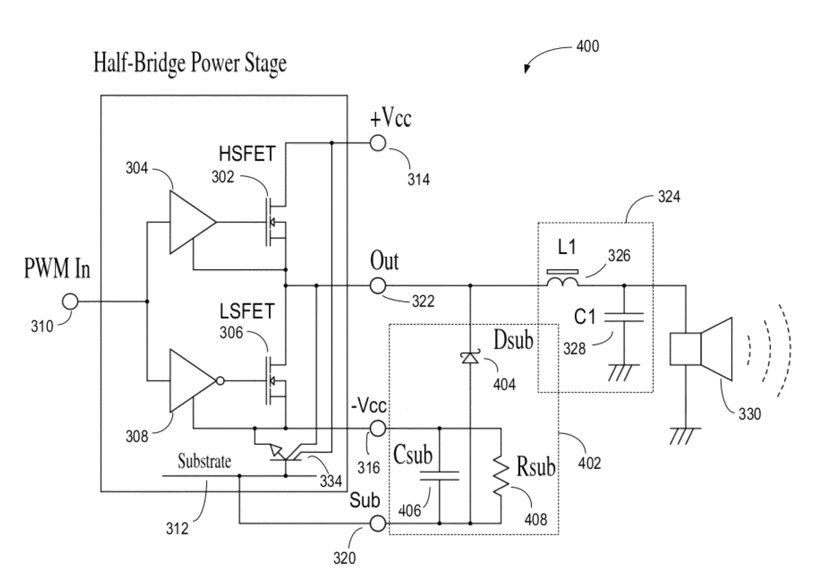
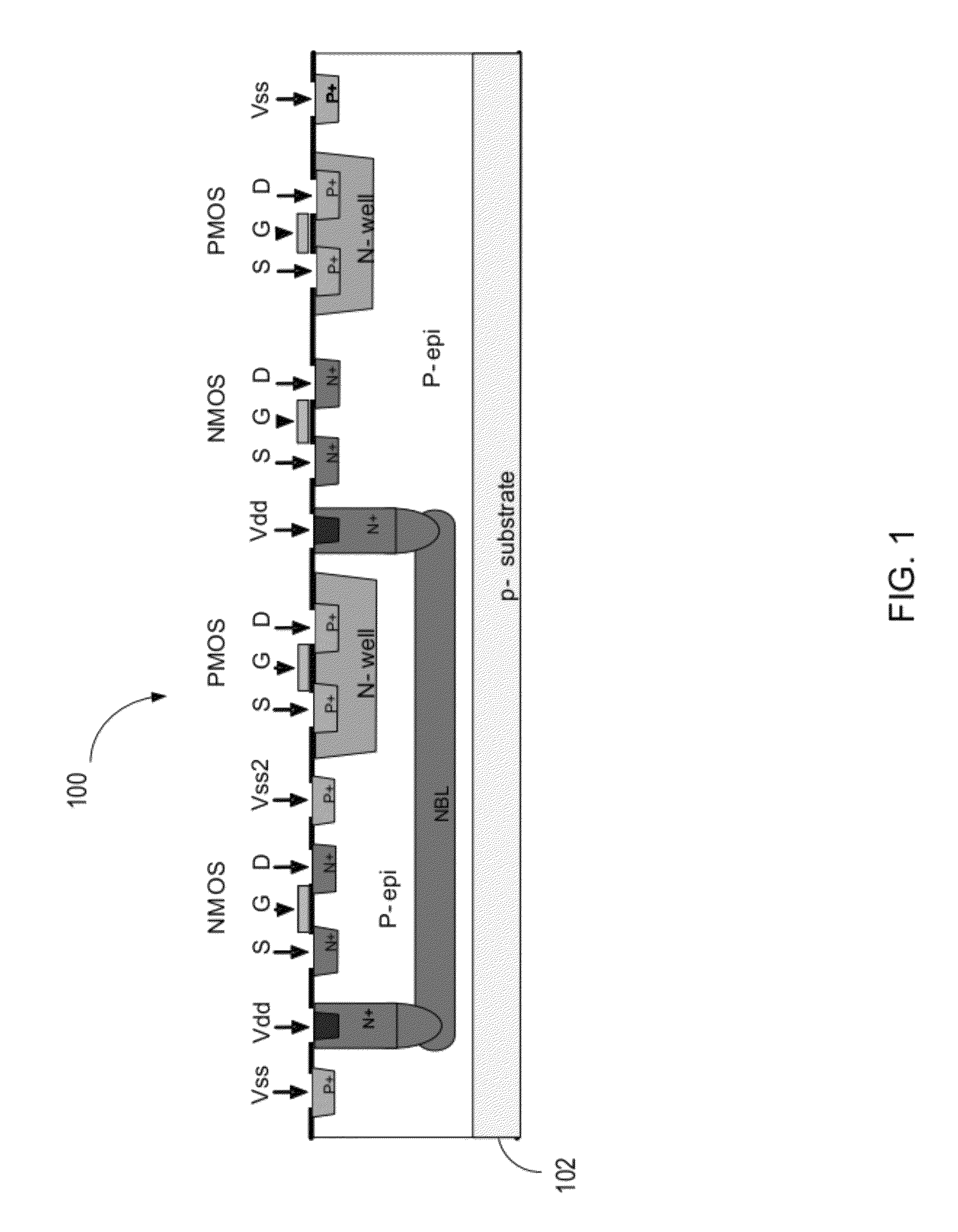
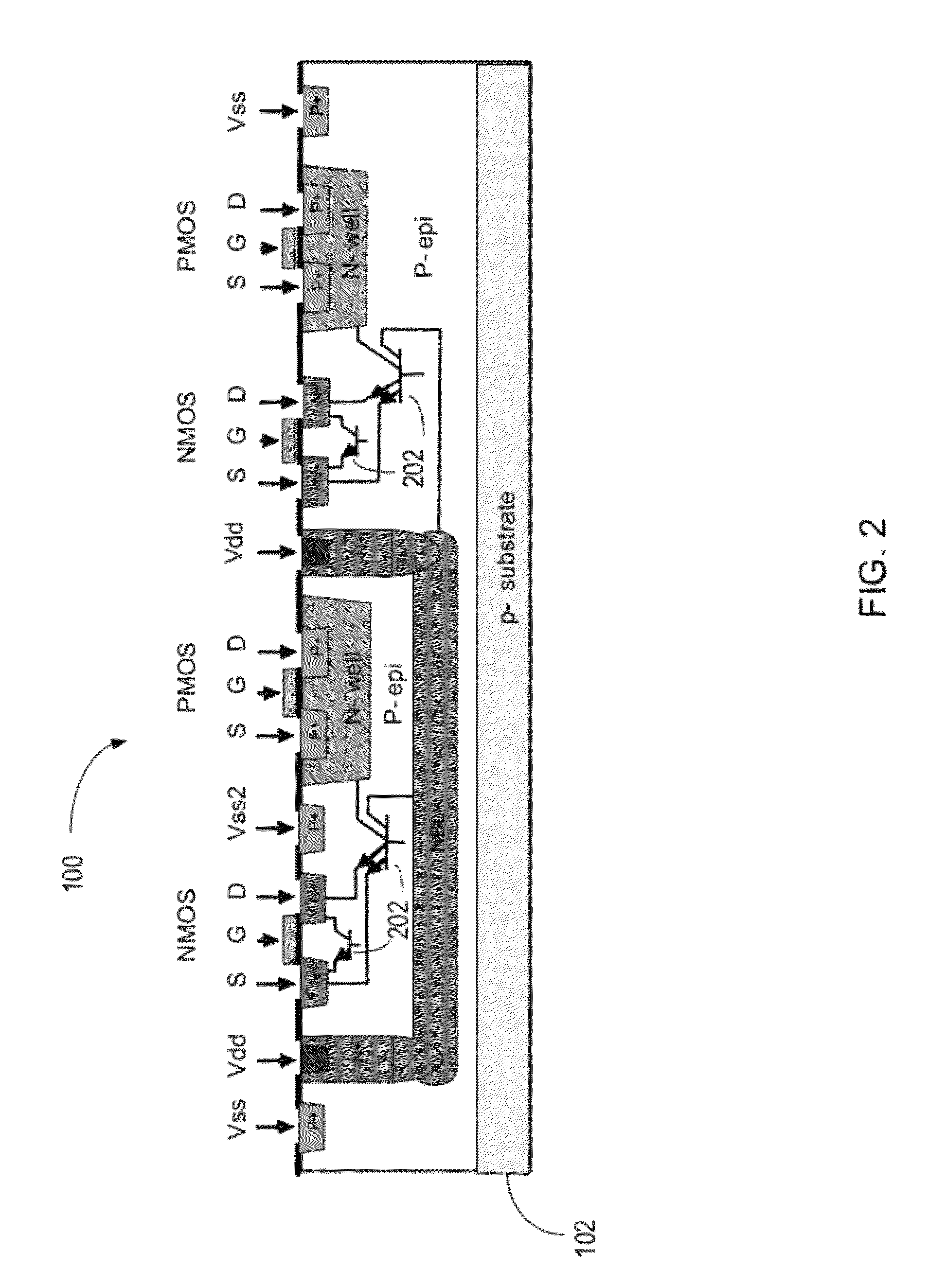
[0020]FIG. 1 is an example architecture for an integrated circuit (IC) 100 incorporated in a semiconductor 102, such as a complimentary metal oxide semiconductor (CMOS) power IC. The example power IC is built upon a lightly doped P-type substrate using more highly doped N-wells to confine switching devices, such as P-channel MOSFETs, built upon the same substrate. In other examples, the switching devices may be other devices, such as PNP bipolar junction transistors (BJT), an insulated gate bipolar transistor (IGBT), a thyristor, or any other form of power transistor, mechanism or device included in an integrated circuit and capable of transitioning between a conducting and a non-conducting state. Although the term “MOSFETS” is used in the following discussion, it should be understood that the switching devices are not limited to MOSFET switching devices. The N-wells could be biased, such as by a power supply, to be more positively biased than any circuitry contained within the IC 1...


PUM


Abstract

An amplifier system for a power converter includes at least a first switching device and a second switching device formed in an integrated circuit in a substrate of a semiconductor. The first and second switching devices may be formed in a half bridge configuration and may be cooperatively switchable to generate an amplified output signal on an output node of the semiconductor. A resistor and a capacitor may be coupled in parallel between a power supply input node and a substrate node included in the semiconductor. The capacitor may be selectively charged to a de-biasing voltage during a switching cycle of the first and second switching devices to reverse bias a parasitic switching device appearing in the integrated circuit.

Description

BACKGROUND OF THE INVENTION[0001]1. Technical Field[0002]This invention relates to power converters, and more particularly to an amplifier system in a power converter that reduces parasitic switching device activity.[0003]2. Related Art[0004]Integrated circuits deploying power electronics and associated circuitry enable cost effective solutions to complex problems in power management. Having thousands of active devices and their interconnections built into one monolithic semiconductor element makes for very efficient systems packaging with a minimum of materials and unreliable connections.[0005]The principle limitations of such devices come in the form of not being able to store large amounts of energy (capacitor and inductor sizes are limited) and the intimate placement of multiple devices within one assembly leads to unintended signals (currents) being coupled from high current members to other signal portions of the circuitry. Parasitic elements such as unintended bipolar transis...

Claims


Application Information

Patent Timeline
Patent Type & Authority Patents(United States)
IPC IPC(8): H03F3/217H03F3/36
CPCH01L21/823892H01L27/0629H03F3/2173H03F1/523H01L27/0921H02M3/335H03F3/217
Inventor STANLEY, GERALD R.
Owner HARMAN INT IND INC
Why Eureka
Try Eureka