Light emitting device and method for manufacturing the same

a technology manufacturing methods, which is applied in the manufacture of semiconductor/solid-state devices, semiconductor devices, electrical apparatus, etc., can solve the problems of deteriorating reliability reducing the life span deteriorating the optical efficiency of light emitting devices, so as to achieve stable operation voltage and stab operation

Active Publication Date: 2012-10-16
SUZHOU LEKIN SEMICON CO LTD
View PDF30 Cites 7 Cited by
  • Summary
  • Abstract
  • Description
  • Claims
  • Application Information

AI Technical Summary

Benefits of technology

[0009]Embodiments provide a light emitting device that can remove or reduce a current concentration phenomenon and a method for manufacturing the same.
[0010]Embodiments provide a light emitting device that can be driven at a stable operation voltage and be stably operated without the deterioration in the light intensity and a method for manufacturing the same.

Problems solved by technology

When this phenomenon occurs, the operating voltage of the light emitting device is raised, the life span of the light emitting device is decreased, and reliability of the light emitting device is deteriorated.
Also, as the light is generated mainly from the active layer on the lower side of the first electrode layer, the generated light is not completely output to the external of the light emitting device but is reflected on the first electrode layer to be absorbed by the light emitting device, thereby deteriorating the optical efficiency of the light emitting device.

Method used


Image

  • Light emitting device and method for manufacturing the same
  • Light emitting device and method for manufacturing the same
  • Light emitting device and method for manufacturing the same

Examples


first embodiment

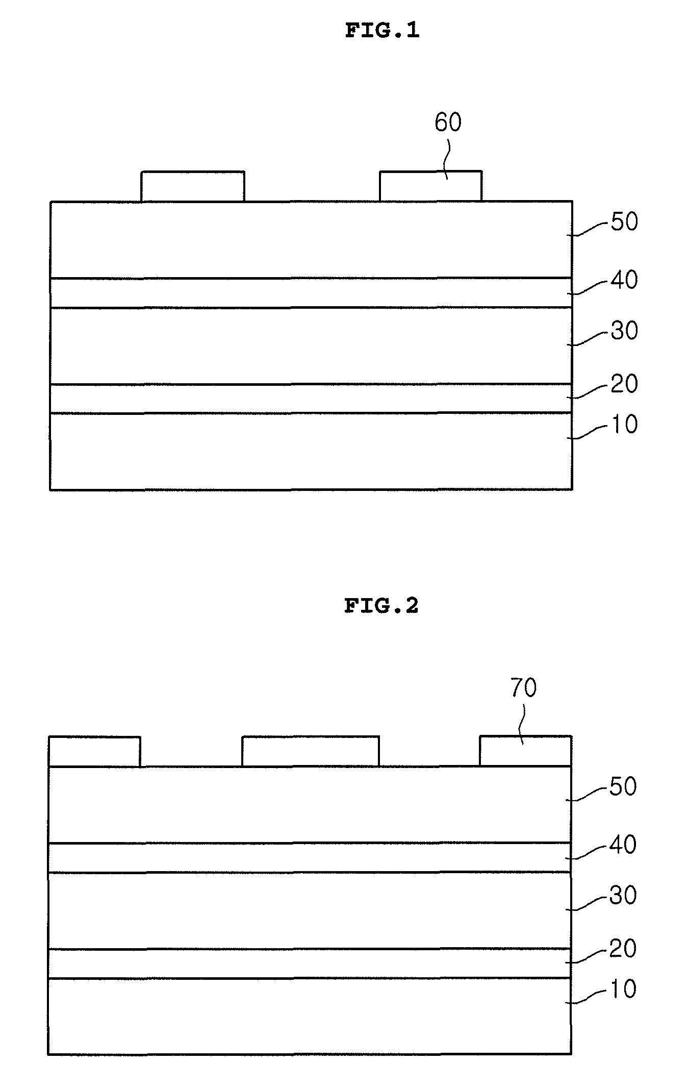
[0028]FIGS. 1 to 5 are diagrams explaining a light emitting device and a method for manufacturing the same.

[0029]First, referring to FIG. 5, the light emitting device according to the first embodiment includes a second electrode layer 90, one or more current blocking layers 70 selectively formed on the second electrode layer 90, a second conductive type semiconductor layer 50 on the second electrode layer 90 and the current blocking layer(S) 70, an active layer 40 and a first conductive type semiconductor layer 30 formed on the active layer 40, and a first electrode layer 100 formed on the first conductive type semiconductor layer 30. All the components of the light emitting device are operatively coupled and configured.

[0030]The current blocking layer(s) 70 are formed between the second electrode layer 90 and the second conductive type semiconductor layer 50, thereby changing the path of current flowing in the light emitting device.

[0031]Each current blocking layer 70 includes a m...

second embodiment

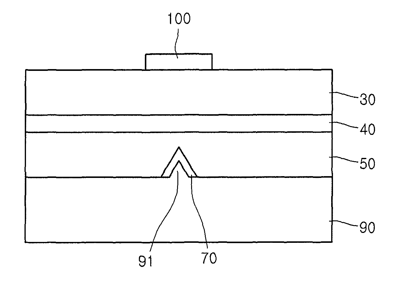
[0071]FIG. 6A is a diagram explaining a light emitting device according to a

[0072]When explaining the light emitting device according to the second embodiment, the description overlapped with the light emitting device according to the first embodiment will be omitted.

[0073]Referring to FIG. 6A, the light emitting device according to the second embodiment includes a second electrode layer 90 that includes a projection part 91, a current blocking layer 70 formed on the projection part 91, a second conductive type semiconductor layer 50 formed on the second electrode layer 90 and the current blocking layer 70, an active layer 40 formed on the second conductive type semiconductor layer 50, a first conductive type semiconductor layer 30 formed on the active layer 40, and a first electrode layer 100 formed on the first conductive type semiconductor layer 30.

[0074]The current blocking layer 70 is formed between the second electrode layer 90 and the second conductive semiconductor layer 50,...

third embodiment

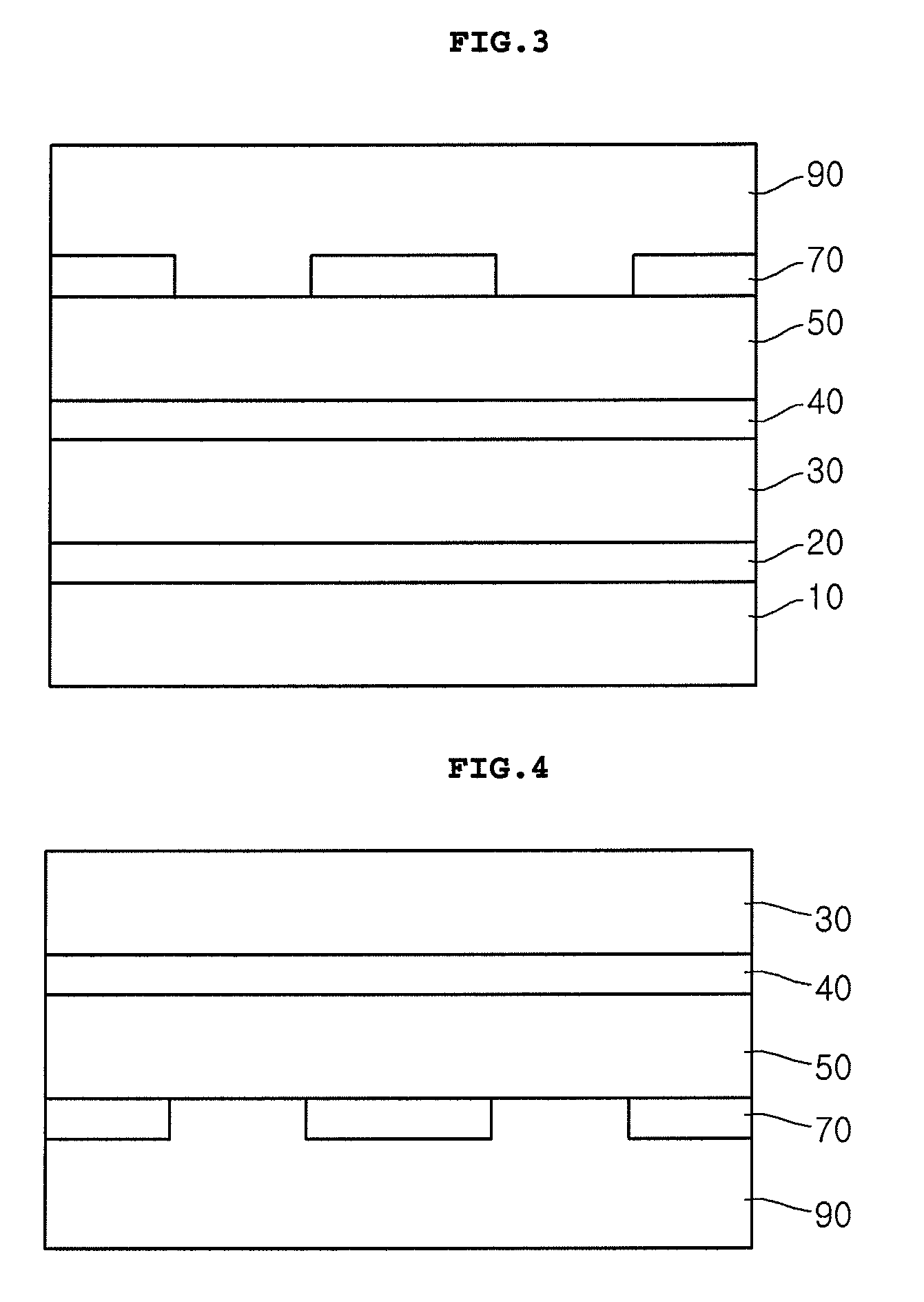
[0082]FIG. 7 is a diagram explaining a light emitting device according to a

[0083]When explaining the light emitting device according to the third embodiment, the description overlapped with the light emitting device according to the first embodiment and the second embodiment will be omitted.

[0084]Referring to FIG. 7, the light emitting device according to the third embodiment has current blocking layers that are a combination of the current blocking layers of the first and second embodiments.

[0085]The current blocking layers 70 are formed on a central portion and peripheral portion(s) of the second electrode layer 90. Similarly, a projection part 91 is formed on the central portion of the second electrode layer 90 to be overlapped with (or correspond with) the first electrode layer 100 in the vertical direction, and the current blocking layer 70 is formed on the projection part 91.

[0086]The current blocking layer 70 formed on the central portion of the second electrode layer 90 is f...


PUM


Abstract

A light emitting device according to an embodiment includes a second electrode layer comprising at least one projection part; at least one current blocking layer on the projection part of the second electrode layer; a second conductive type semiconductor layer on the second electrode layer and the current blocking layer; an active layer on the second conductive type semiconductor layer; a first conductive type semiconductor layer on the active layer; and a first electrode layer on the first conductive type semiconductor layer, at least a portion of the first electrode layer corresponding with the current blocking layer in a vertical direction.

Description

CROSS-REFERENCE TO RELATED APPLICATIONS[0001]The present application claims priority under 35 U.S.C. 119 and 35 U.S.C. 365 to Korean Patent Application No. 10-2008-0116751 filed on Nov. 24, 2008, which is hereby incorporated by reference in its entirety.BACKGROUND OF THE INVENTION[0002]Embodiments relate to a light emitting device and a method for manufacturing the same.[0003]Recently, an apparatus using a light emitting diode (LED) has been widely studied as a light emitting device.[0004]The LED is an apparatus to convert electrical signals to light using characteristics of a semiconductor, wherein a first conductive type semiconductor layer, an active layer, and a second conductive type semiconductor are stacked and then power is applied to the stacked structure so that light is emitted from the active layer. The first conductive type semiconductor layer may be an n-type semiconductor layer and the second conductive type semiconductor layer may be a p-type semiconductor layer. Alt...

Claims


Application Information

Patent Timeline
Patent Type & Authority Patents(United States)
IPC IPC(8): H01L33/00H01L21/00
CPCH01L33/145H01L33/60
Inventor HWANG, SUNG MINCHO, HYUN KYONGPARK, GYEONG GEUN
Owner SUZHOU LEKIN SEMICON CO LTD
Why Eureka
Try Eureka