
Light emitting apparatus, method for manufacturing the light emitting apparatus, electronic device and cell phone device

a technology of light emitting apparatus and manufacturing method, which is applied in the manufacture of electrode systems, electric discharge tubes/lamps, and discharge tubes luminescnet screens, etc., to achieve the effect of reducing resin viscosity, reducing resin viscosity, and increasing specific gravity

Active Publication Date: 2012-10-16
SHARP KK
View PDF24 Cites 17 Cited by
  • Summary
  • Abstract
  • Description
  • Claims
  • Application Information

AI Technical Summary

Benefits of technology

The present invention provides a light emitting apparatus for camera lighting in electronic devices, such as cell phones, that includes a phosphor in the encapsulating resin section and is capable of emitting white light while maintaining the light emitting efficiency. The surface resin layer is a different color from the encapsulating resin section, which does not yellow the appearance of the device. The light emitting apparatus includes a blue color LED and an optical diffusion material that reflects visible light ranging between a blue color and a red color. The optical diffusion material can be particles of about 2 μm-5 μm in size or one of organic filler, fused silica, or titanium oxide. The color of the surface resin layer can be white, a color ranging between green and red, or a whitish light color ranging between green and red. The light emitting apparatus can be used in electronic devices such as cell phones and cameras.

Problems solved by technology

The conventional technique described above, however, has the following problems.

Method used


Image

  • Light emitting apparatus, method for manufacturing the light emitting apparatus, electronic device and cell phone device
  • Light emitting apparatus, method for manufacturing the light emitting apparatus, electronic device and cell phone device
  • Light emitting apparatus, method for manufacturing the light emitting apparatus, electronic device and cell phone device

Examples


example 1

[0153]FIG. 9 is a longitudinal cross sectional view showing a light emitting apparatus according to Example 1 of Embodiment 3 of the present invention. Further, the same reference numerals are provided for those structural members which have the same functional effects as those in FIG. 2.

[0154]In FIG. 9, a light emitting apparatus 15 according to Example 1 has an encapsulating resin section 3, the encapsulating resin section being divided into a layer substantially including a phosphor 13 and a layer substantially including an optical diffusion material 14 as a surface resin layer from the side closer to an LED chip 6 as a light emitting device. Alternatively, the encapsulating resin section is divided into a layer substantially including the phosphor 13, an intermediate layer including the phosphor 13 and an optical diffusion material 14 intermingled together, and a layer substantially including the optical diffusion material 14 as the surface resin layer from the side closer to th...

example 2

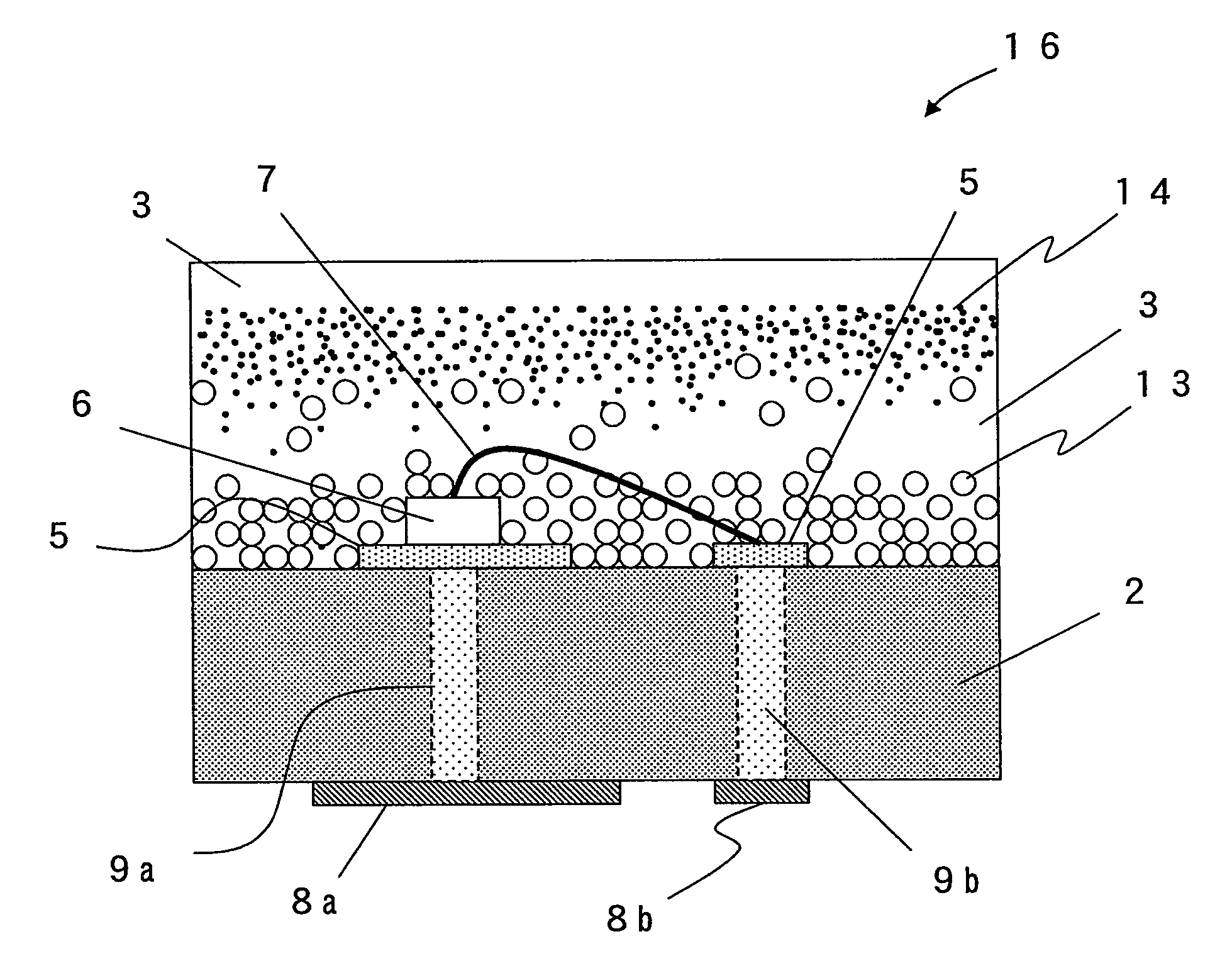
[0159]FIG. 10 is a longitudinal cross sectional view showing an exemplary essential structure according to a light emitting apparatus 16 of Example 2 of Embodiment 3 according to the present invention. Further, the same reference numerals are provided for those structural members which have the same functional effects as those in FIG. 2.

[0160]In FIG. 10, the light emitting apparatus 16 according to Example 2 has an encapsulating resin section 3, the encapsulating resin section being divided, from the side closer to the light emitting device, into a layer substantially including a phosphor 13, a layer including the phosphor 13 and an optical diffusion material 14 intermingled together, a layer substantially including the optical diffusion material 14, and a layer only with the resin material for the encapsulating resin section 3 (a layer which does not include the phosphor 13 or the optical diffusion material 14).

[0161]With the structure described above, the manufacturing method of t...

example 3

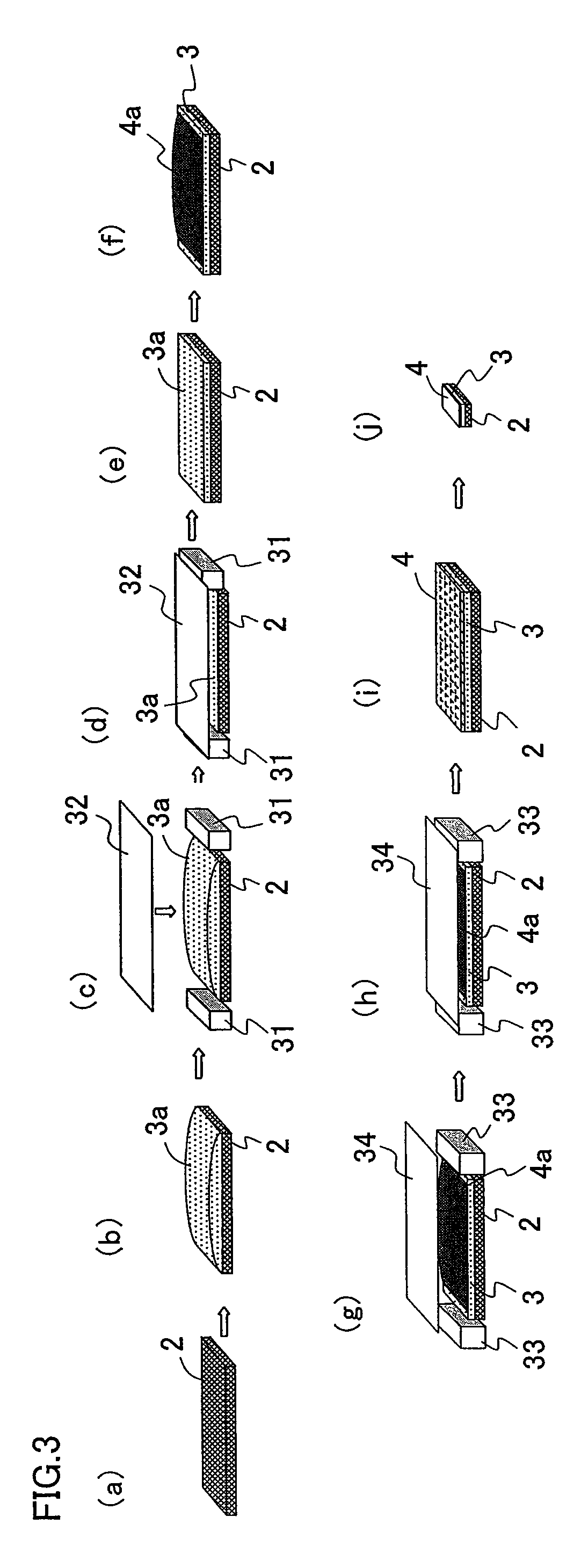
[0169]FIGS. 11(a) and 11(b) are respectively longitudinal cross sectional views each showing an exemplary structure in the middle of the manufacturing step of the light emitting apparatus according to Example 3 of the present invention. FIG. 12 is a longitudinal cross sectional view showing an exemplary essential structure of the light emitting apparatus according to Example 3 of the present invention. Further, the same reference numerals are provided for those structural members which have the same functional effects as those in FIG. 2.

[0170]As shown in FIG. 12, a light emitting apparatus 17 of Example 3 has an encapsulating resin section 3 which is divided from the side closer to a light emitting device 6 into a layer substantially including a phosphor 13, and a layer substantially including the optical diffusion material 14, which functions as a surface resin layer.

[0171]According to the manufacturing method of the light emitting apparatus 17 of Example 3 with the structure descr...


PUM


Abstract

A light emitting apparatus is provided, and the light emitting apparatus has a light emitting device mounted on a substrate or a resin package where a substrate surface or the resin package is resin-encapsulated by an encapsulating resin section added with a phosphor in such a manner to cover the light emitting device. A surface resin layer of a different color from that of the encapsulating resin section is provided on a surface side of the encapsulating resin section.

Description

[0001]This Nonprovisional application claims priority under 35 U.S.C. §119(a) on Patent Application No. 2007-149815 filed in Japan on Jun. 5, 2007, the entire contents of which are hereby incorporated by reference.BACKGROUND OF THE INVENTION[0002]1. Field of the Invention[0003]The present invention relates to a light emitting apparatus equipped with a light emitting device, such as an LED, and resin-encapsulated thereon; a method for manufacturing the light emitting apparatus; an electronic device equipped with the light emitting apparatus as camera lighting therein, such as a digital camera (e.g., digital video camera and digital still camera), a door intercom camera, a camera for television telephone, and a camera equipped in a cell phone; and a cell phone device with the camera equipped in a cell phone.[0004]2. Description of the Related Art[0005]LEDs have been conventionally used as a flash for camera lighting of a cell phone device, and References 1 and 2, for example, disclose...

Claims


Application Information

Patent Timeline
Patent Type & Authority Patents(United States)
IPC IPC(8): H05B33/14
CPCC09K11/02C09K11/0883C09K11/7721C09K11/7734H01L33/50H01L33/46H01L2224/48091H01L2933/0091H01L2924/00014C09K11/77342
Inventor OHTA, MASAYUKIKONISHI, MASAHIROTAKENAKA, YASUJI
Owner SHARP KK
Learn More