Touch panel and electronic device using the same

a technology of electronic devices and touch panels, applied in the direction of instruments, computing, electric digital data processing, etc., can solve the problems of not expressing the absolute position of the touch panel or the member, the adhesion strength of the adhesive layer may not be sufficient in a certain width x, and it is difficult to find appropriate processing conditions, etc., to achieve the effect of easy formation of the protective layer, easy controllability and quality, and enhanced manufacturing yield of the touch panel

Inactive Publication Date: 2005-03-03
PANASONIC CORP
View PDF6 Cites 101 Cited by
  • Summary
  • Abstract
  • Description
  • Claims
  • Application Information

AI Technical Summary

Benefits of technology

[0060] In this structure, contact of protective layer of FPC and transparent substrate can be avoided, and a wide area of adhesive layer is assured in other region than the vicinity of the FPC, so that a touch panel of narrow marginal edge is realized, while excellent visual recognition, controllability and quality can be easily obtained.
[0061] In other touch panel of the invention, moreover, the distance between the connector and the transparent substance not adhered to the FPC of the first transparent substrate and second transparent substrate is set at 2 mm or more. By coating with a dispenser or the like so as not to contact with the transparent substance not adhered to the FPC of the first transparent substrate and second transparent substrate, it is easier to form the protective layer, and the manufacturing yield of touch panels is enhanced, and a higher quality can be obtained.
[0062] Also in other touch panel of the invention, the projective layer aroun

Problems solved by technology

However, they do not express the absolute position of the touch panel or members or parts composing the touch panel.
That is, it takes much time and labor to find appropriate processing conditions.
When setting of heating and pressing conditions is improper, as shown in FIG. 19, adhesion strength by the adhesive layer may not be sufficient in a certain width X due to effects of step difference portions.
Therefore, from the viewpoint of reduction of number of working processes, the prior art still has many proble

Method used


Image

  • Touch panel and electronic device using the same
  • Touch panel and electronic device using the same
  • Touch panel and electronic device using the same

Examples


first exemplary embodiment

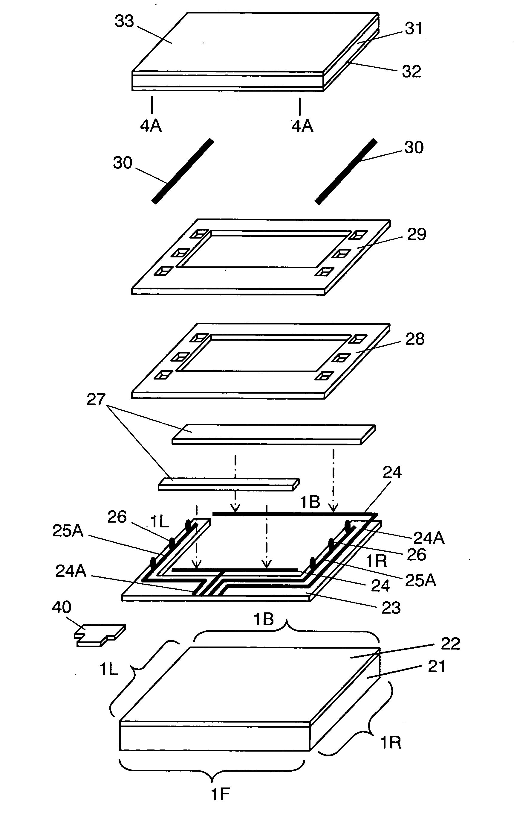
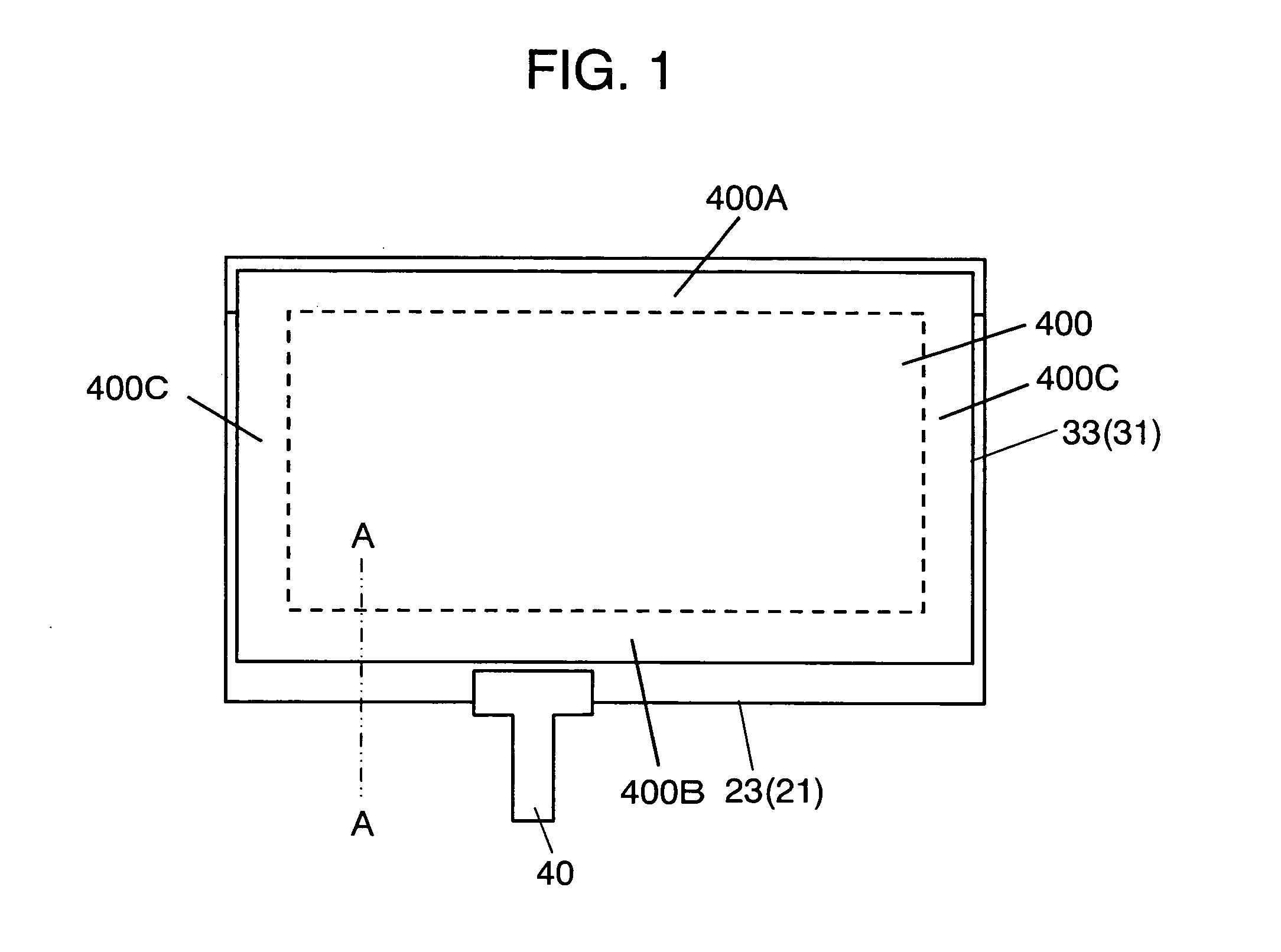
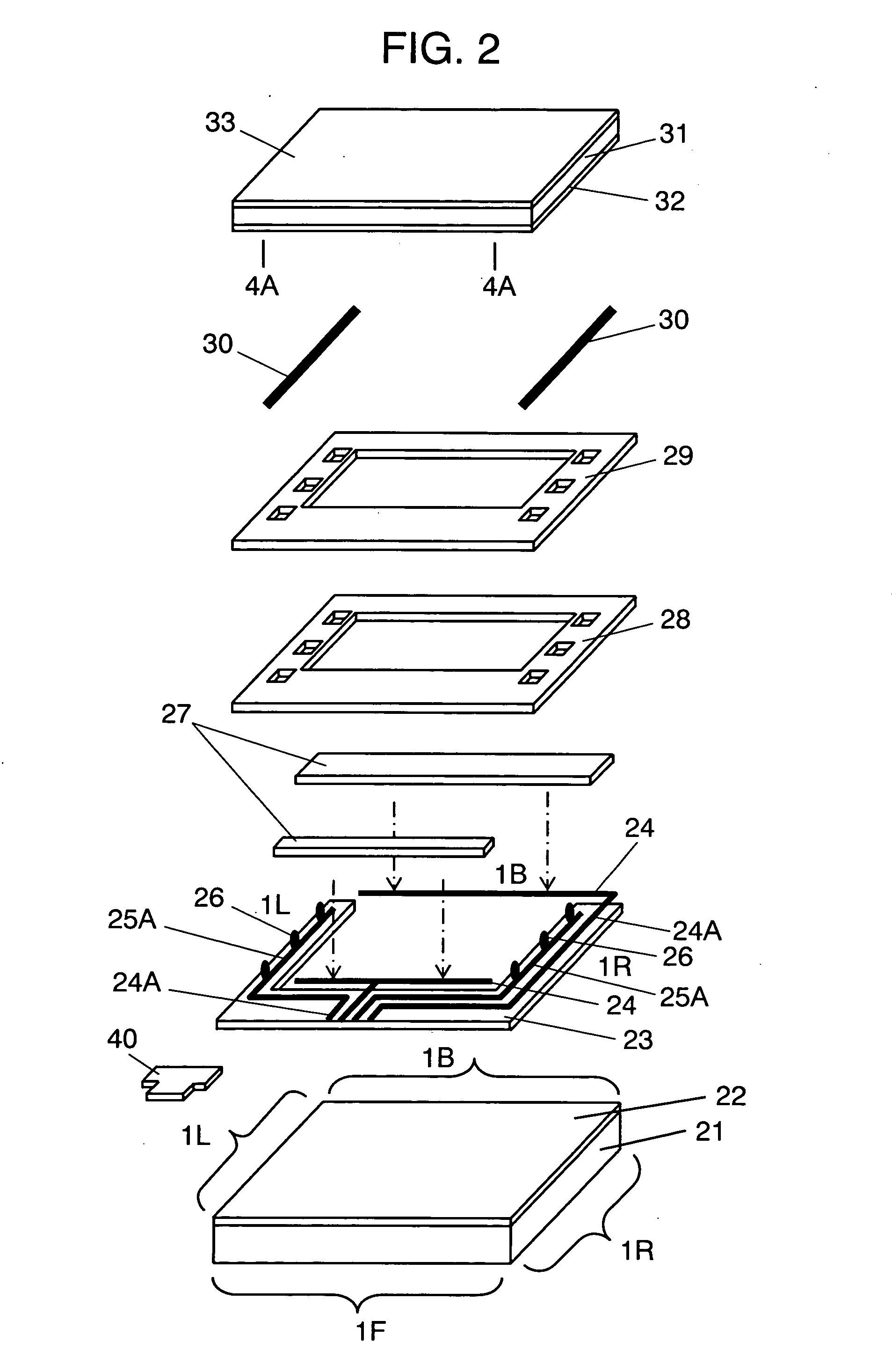
[0086]FIG. 1 is a top view of touch panel in a first exemplary embodiment of the invention, FIG. 2 is its perspective exploded view, and FIG. 3 is a sectional view along line A-A in FIG. 1.

[0087] On the upside of first transparent substrate 21 made of soda glass of rectangular shape, first transparent conductive film 22 of ITO or the like is formed on the entire surface. In touch panel operation region 400 disposed nearly in the center of first transparent conductive film 22, dot spacers 20 of small size made of insulating epoxy resin are formed at specific intervals.

[0088] On the entire downside of second transparent substrate 31 of rectangular shape, second transparent conductive film 32 of ITO is formed. The material of second transparent conductive film 32 is, for example, biaxially drawn polyethylene terephthalate film, and its thickness is 188 μm.

[0089] Second transparent conductive film 32 is disposed oppositely to first transparent substrate 21 and second transparent subs...

second exemplary embodiment

[0138]FIG. 4 is a top view of touch panel in a second exemplary embodiment of the invention, FIG. 5 is its perspective exploded view, FIG. 6 is a sectional view along line B-B in FIG. 4, and FIG. 7 is a sectional view along line C-C in FIG. 4.

[0139] Same parts as in the first exemplary embodiment shown in FIG. 1 to FIG. 3 are identified with same reference numerals, and their explanation is omitted.

[0140] In the touch panel of the second exemplary embodiment, same as in the first exemplary embodiment, first transparent substrate 21 and second transparent substrate 31 are adhered with first transparent conductive film 22 and second transparent conductive film 32 face to face across a specific interval, and adhered and fixed with marginal outer circumferential parts 400A, 400B, and 400C. At the front side, FPC 40 is adhered same as in the first exemplary embodiment.

[0141] Second transparent substrate 31 has, as shown in FIG. 4, a rectangular shape of a nearly same size as first tra...

third exemplary embodiment

[0164]FIG. 8 is a top view of touch panel in a third exemplary embodiment of the invention, and FIG. 9 is its perspective exploded view. As compared with the second exemplary embodiment, the touch panel of the third exemplary embodiment is different in the installation state of FPC 52. Same parts as in the second exemplary embodiment are identified with same reference numerals, and their explanation is omitted.

[0165] In the entire surface of downsize of second transparent substrate 51 made of polyethylene terephthalate, second transparent conductive film 53 is formed, and hard coat layer 54 is formed on the entire surface of its upside. Second transparent substrate 51 has a rectangular shape having no notch or disposing FPC 52. Second transparent substrate 51 is disposed face to face with first transparent substrate 21 so as to overlap in a specified portion on FPC 52 adhered and fixed on first transparent conductive film 22 formed on first transparent substrate 21.

[0166] Same as ...


PUM


Abstract

The invention presents a touch panel disposed at the display screen side of a liquid crystal display device or the like, and excellent in surface smoothness and environmental resistance. In marginal outer circumferential part 400B for adhering and fixing first transparent substrate 21 and second transparent substrate 31 face to face, insulating layer 27 for correction of step difference is disposed in order to make uniform the film thickness. Adhesive layer 29 is disposed on insulating layer 27, and first transparent substrate 21 and second transparent substrate 31 are adhered to each other. As a result, the adhesion fixing state if stabilized, and the adhesion strength is enhanced, and a touch panel suitable for car-mount unit excellent in surface smoothness and environmental resistance can be presented.

Description

FIELD OF THE INVENTION [0001] The present invention relates to a touch panel mounted on a display screen side of a liquid crystal display device or the like capable of entering coordinate positions by pressing operation by pen or finger corresponding to the display item or display content, and an electronic device using the same. BACKGROUND OF THE INVENTION [0002] Touch panels capable of entering coordinate positions by pressing operation by pen or finger corresponding to the display item or display content are widely used recently in electronic devices including portable devices. [0003] Touch panels are available in various types. A touch panel of resistance film analog type most widely used at the present is explained below by referring to the drawings. FIG. 16 to FIG. 19 show a touch panel in a first prior art. FIG. 21 and FIG. 22 show a touch panel in a second prior art. [0004] In the drawings shown below, for the ease of understanding of the structure of touch panel and for the...

Claims


Application Information

Patent Timeline
IPC IPC(8): G06F3/033G06F3/048
CPCG06F3/0488G06F3/045
Inventor NAKANISHI, AKIRAFUJII, SHIGEYUKITAKABATAKE, KENICHI
Owner PANASONIC CORP
Why Eureka
Try Eureka