

Pseudo page mode memory architecture and method
a memory architecture and page mode technology, applied in the field of memory integrated circuits, can solve the problems of slow programming time, higher testing cost, and various limitations of conventional non-volatile memory, and achieve the effects of low programming time, cost benefit of dram, and higher testing cos
- Summary
- Abstract
- Description
- Claims
- Application Information
AI Technical Summary
Benefits of technology
Problems solved by technology
Method used
Image

Examples
Embodiment Construction
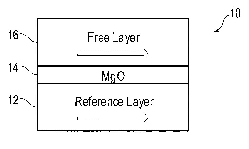
[0038]FIG. 6 is a block diagram of an MRAM array and associated writing and reading circuitry 100, hereinafter alternatively referred to as MRAM 100, in accordance with one embodiment of the present invention. MRAM 100 includes a multitude of array blocks selected by column select drivers, a multitude of global write, a multitude of global sense amp (SA), a multitude of global word line (GWL) circuits, and a control circuit. Each block may include an array of MRAM cells (memory array tile, or MAT) 102 whose rows are selected by one or more sub word line (SWL) circuits, and whose columns are selected by one or more local column select circuits (LCS) 104. The corners of each block include an array gap area 110 to be described in further detail below. In some embodiments, MRAM 100 also includes a register block 107 for reading and / or writing operations.
[0039]FIG. 7 is a schematic diagram 200 of portions of MRAM 100, in accordance with one embodiment of the present invention. Schematic ...
PUM
| Property | Measurement | Unit |
|---|---|---|
| Vpp programming voltage | aaaaa | aaaaa |
| voltages | aaaaa | aaaaa |
| voltages | aaaaa | aaaaa |
Abstract
Description
Claims
Application Information