
NAND flash module replacement for DRAM module
a technology of dram module and flash module, applied in the field of memory module design, to achieve the effect of the most efficien
- Summary
- Abstract
- Description
- Claims
- Application Information
AI Technical Summary
Benefits of technology
Problems solved by technology
Method used
Image

Examples
Embodiment Construction
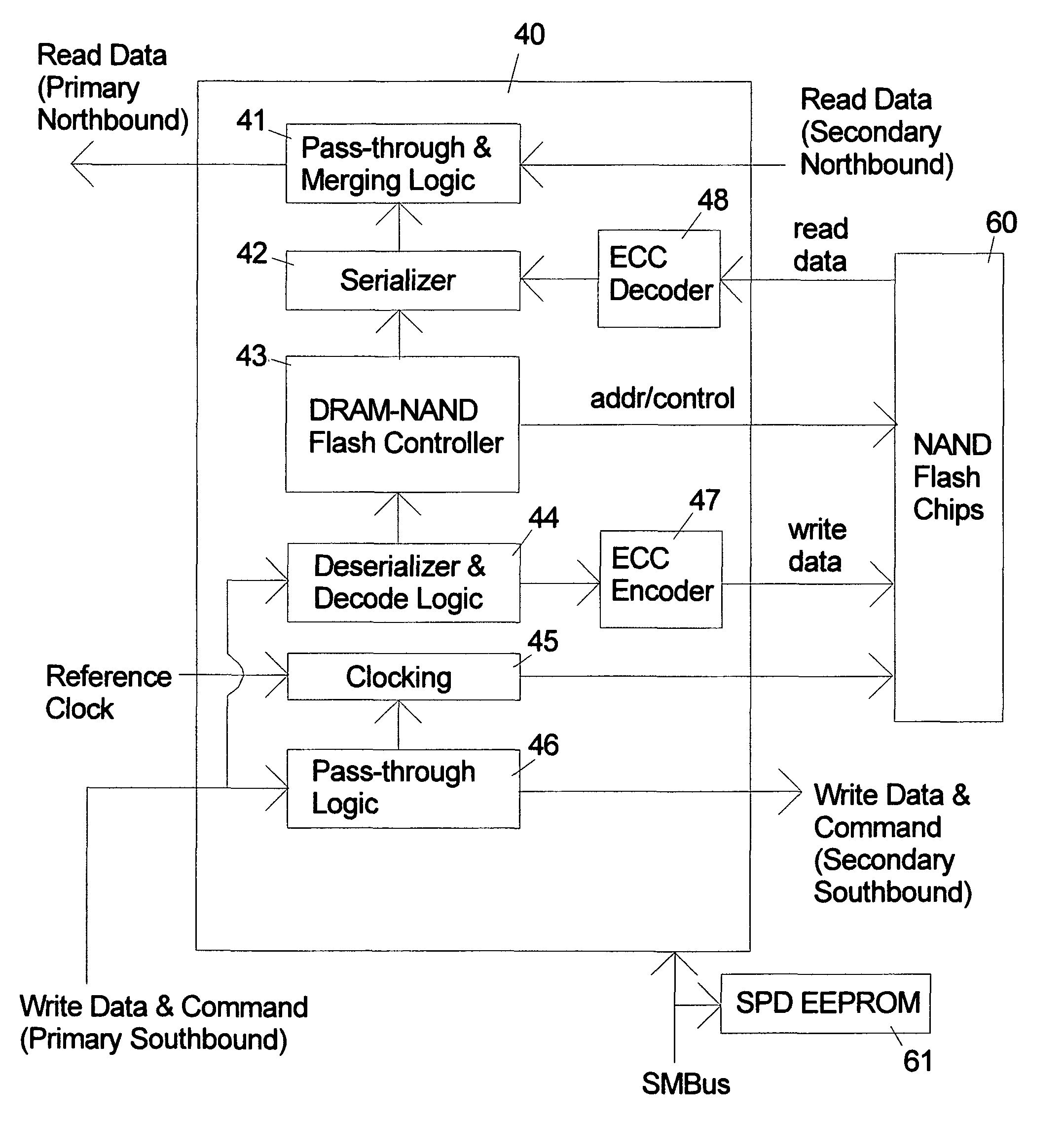
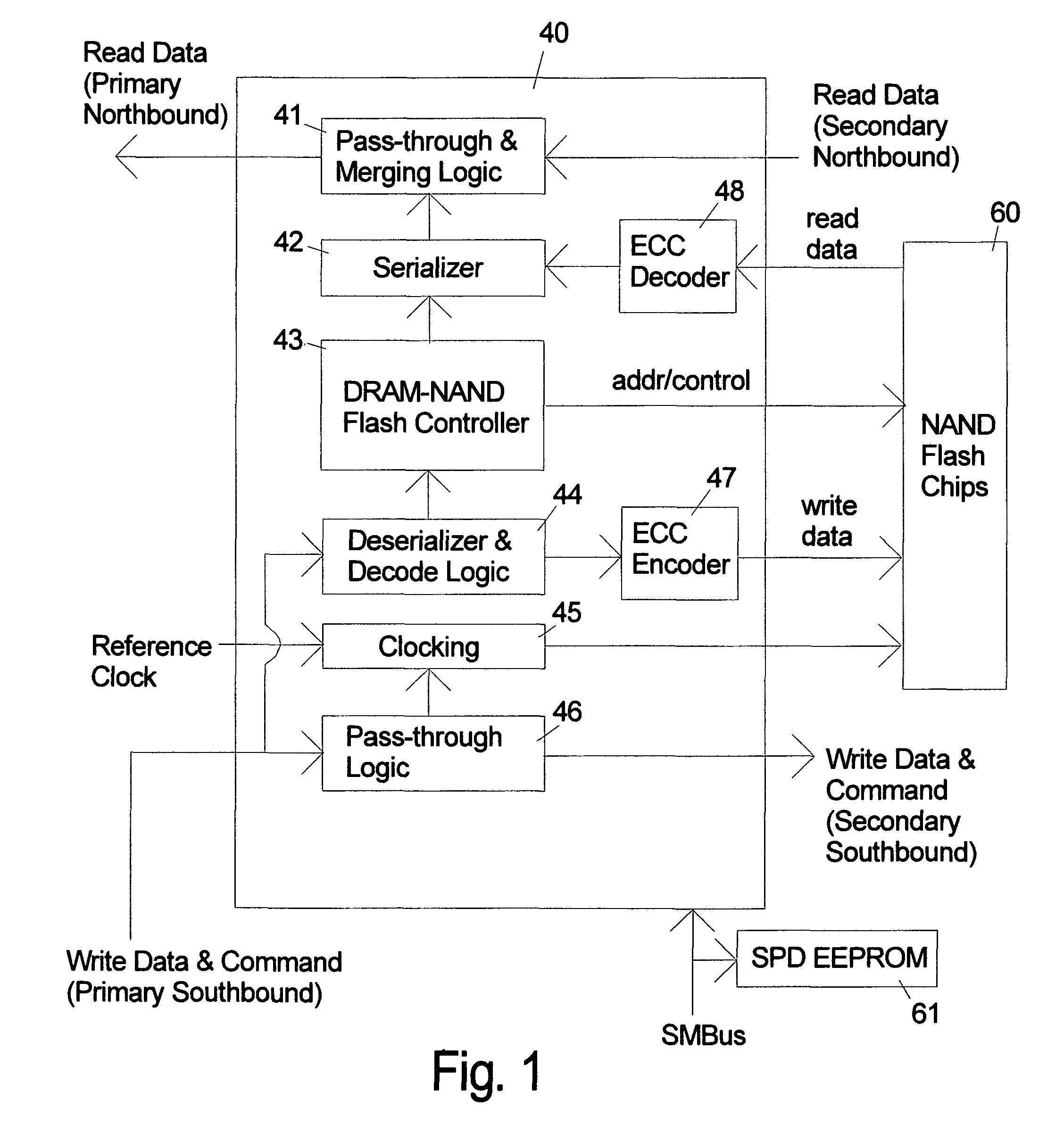
[0014]A preferred embodiment of the invention is a NAND flash based memory module that is plug compatible with existing DRAM and DIMM modules to enable NAND flash to be included in systems where DRAMs and DIMMs were previously used. Because NAND flash is slower, application workload may preclude its use in some systems. However, in large storage controllers for disk drives, the DRAM memory arrays are accessed in large blocks, frequently doing 16K-64K transfers at a time which makes the use of flash memory feasible. Likewise, most printer controllers do not require high data rates, so a flash memory module according to the invention could be used effectively.
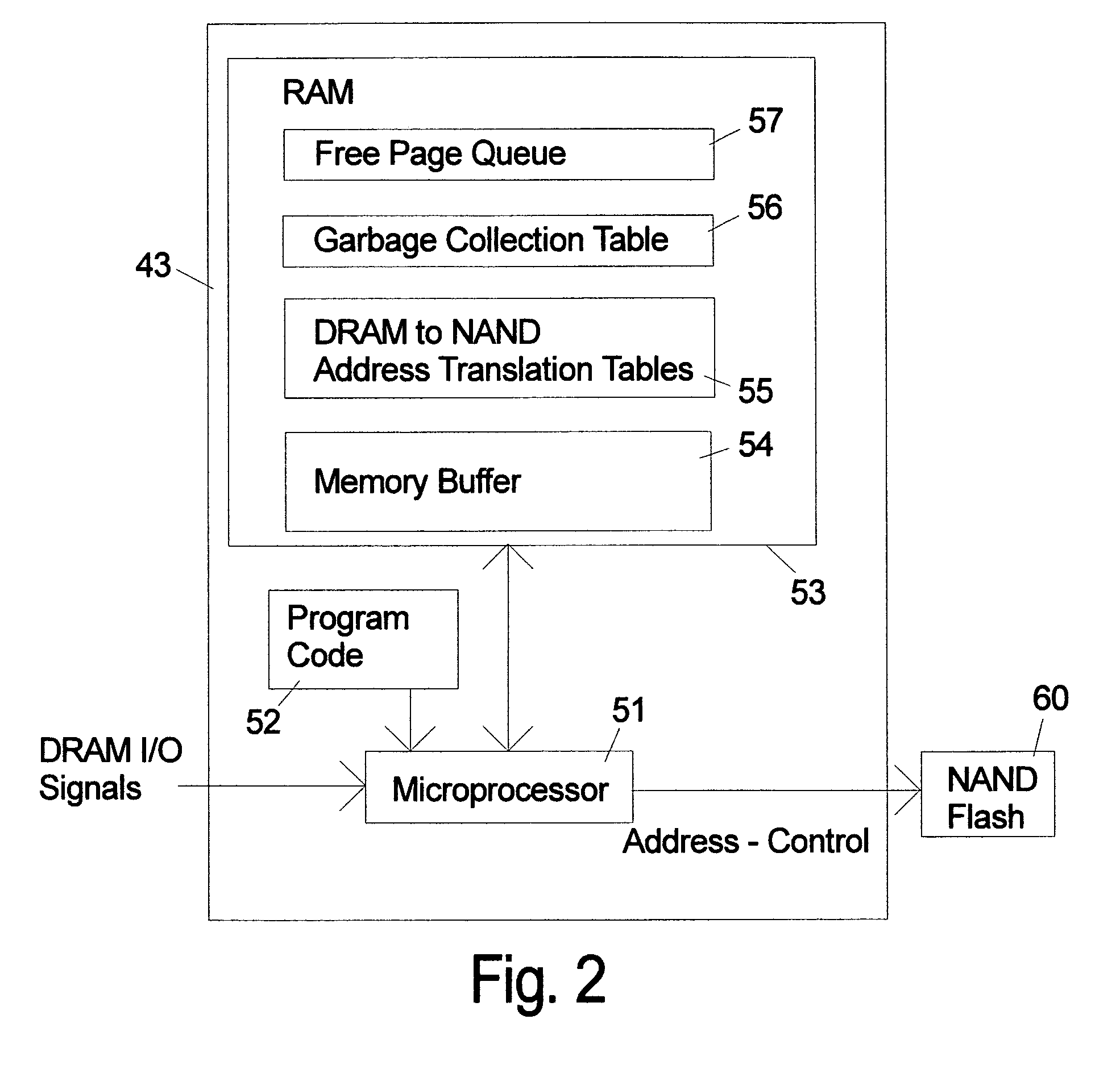
[0015]Buffering architecture allows the output to be delayed while the appropriate block of data is read from the flash at less than DRAM speed. In general, where asynchronous interfaces are used from the host to the memory target, the system according to the invention can supply data from the slower NAND flash without causing sy...
PUM
 Abstract
Description
Claims
Application Information