

Semiconductor light emitting device
a technology of semiconductor devices and light emitting devices, which is applied in the direction of semiconductor devices, lasers, semiconductor lasers, etc., can solve the problems of difficult to realize current injection in a microcavity structure, and not practical devices
- Summary
- Abstract
- Description
- Claims
- Application Information
AI Technical Summary
Benefits of technology
Problems solved by technology
Method used
Image

Examples
Embodiment Construction
[0041]Hereinafter, preferred embodiments of a semiconductor light emitting device according to the present invention will be described in detail with reference to the drawings. In the description of the drawings, the same components are attached with the same reference symbols, and overlapping description will be omitted. Moreover, the dimensional ratios in the drawings are not always equal to those in the description.
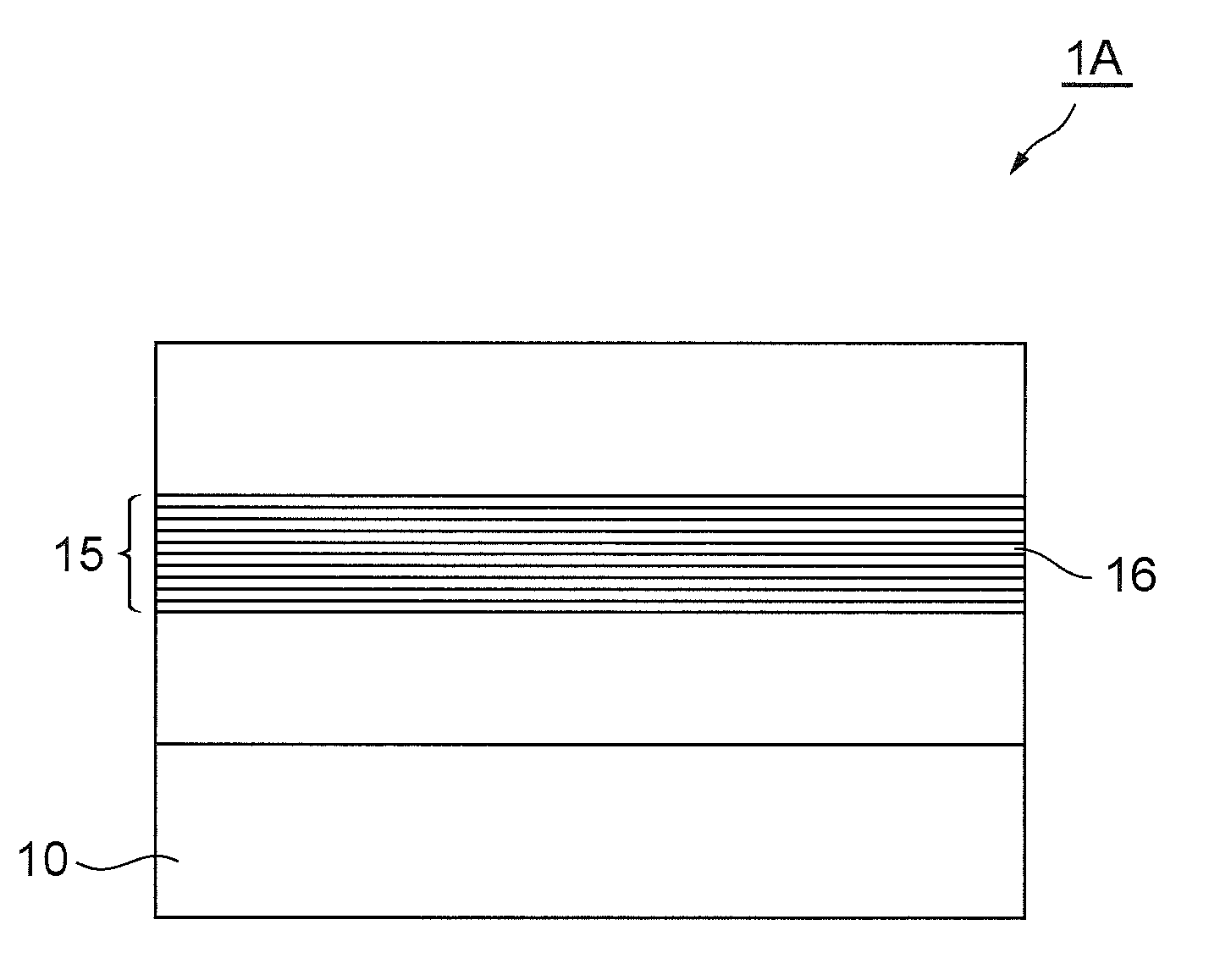
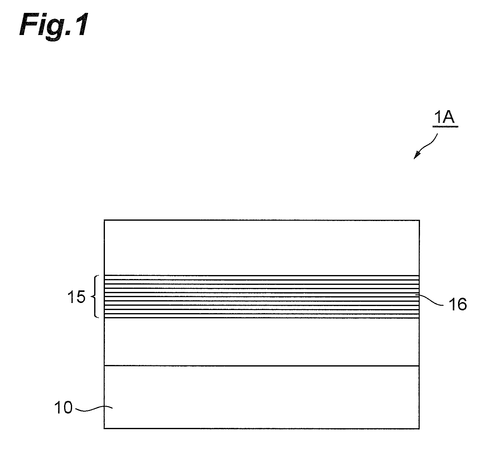
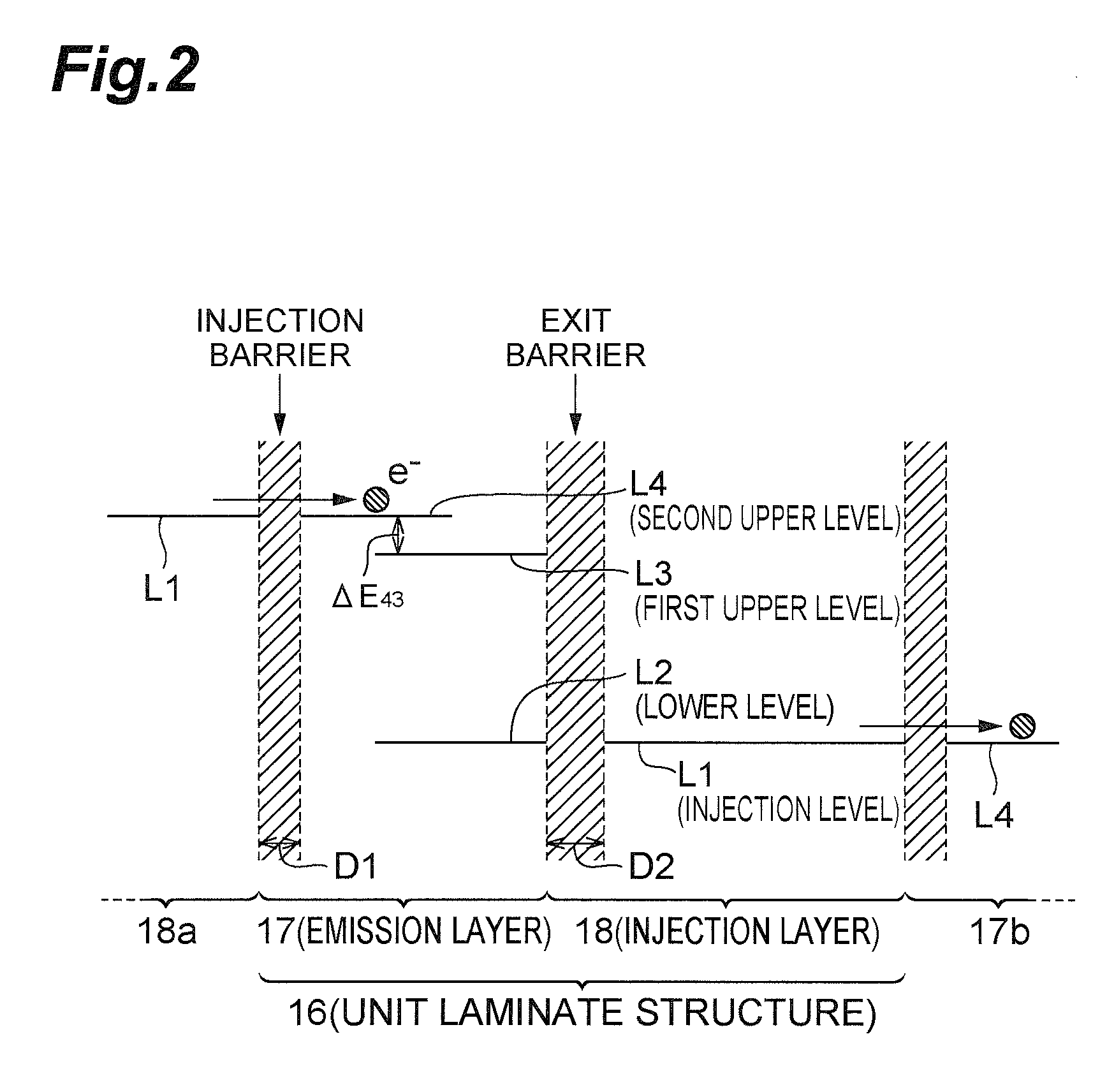
[0042]FIG. 1 is a view schematically showing a basic configuration of a semiconductor light emitting device according to the present invention. A semiconductor light emitting device 1A of the present embodiment is a monopolar type light emitting device which generates light by emission transition using a subband level structure in a semiconductor quantum well structure. This light emitting device 1A is especially configured as a novel semiconductor light emitting device using polaritons, and the emission structure thereof is characterized by a polariton generation stru...
PUM
 Abstract
Description
Claims
Application Information