
Semiconductor light emitting device

a technology of semiconductor devices and light emitting devices, which is applied in the direction of semiconductor devices, lasers, semiconductor lasers, etc., can solve the problems of difficult to realize current injection in a microcavity structure, and not practical devices

Inactive Publication Date: 2011-02-03
HAMAMATSU PHOTONICS KK
View PDF7 Cites 10 Cited by
  • Summary
  • Abstract
  • Description
  • Claims
  • Application Information

AI Technical Summary

Benefits of technology

[0011]The inventors of the present application developed a quantum cascade laser (QCL) as a semiconductor light emitting device using intersubband transition in a quantum well structure (refer to, for example, Patent Documents 2 to 8 for the quantum cascade laser). The quantum cascade laser is a monopolar type laser element which uses a level structure of subbands formed in a semiconductor quantum well structure, and generates light by intersubband electron transition, and realizes high-efficiency and high-output operation by multistage-coupling light emission layers of a quantum well structure in a cascade manner via injection layers.
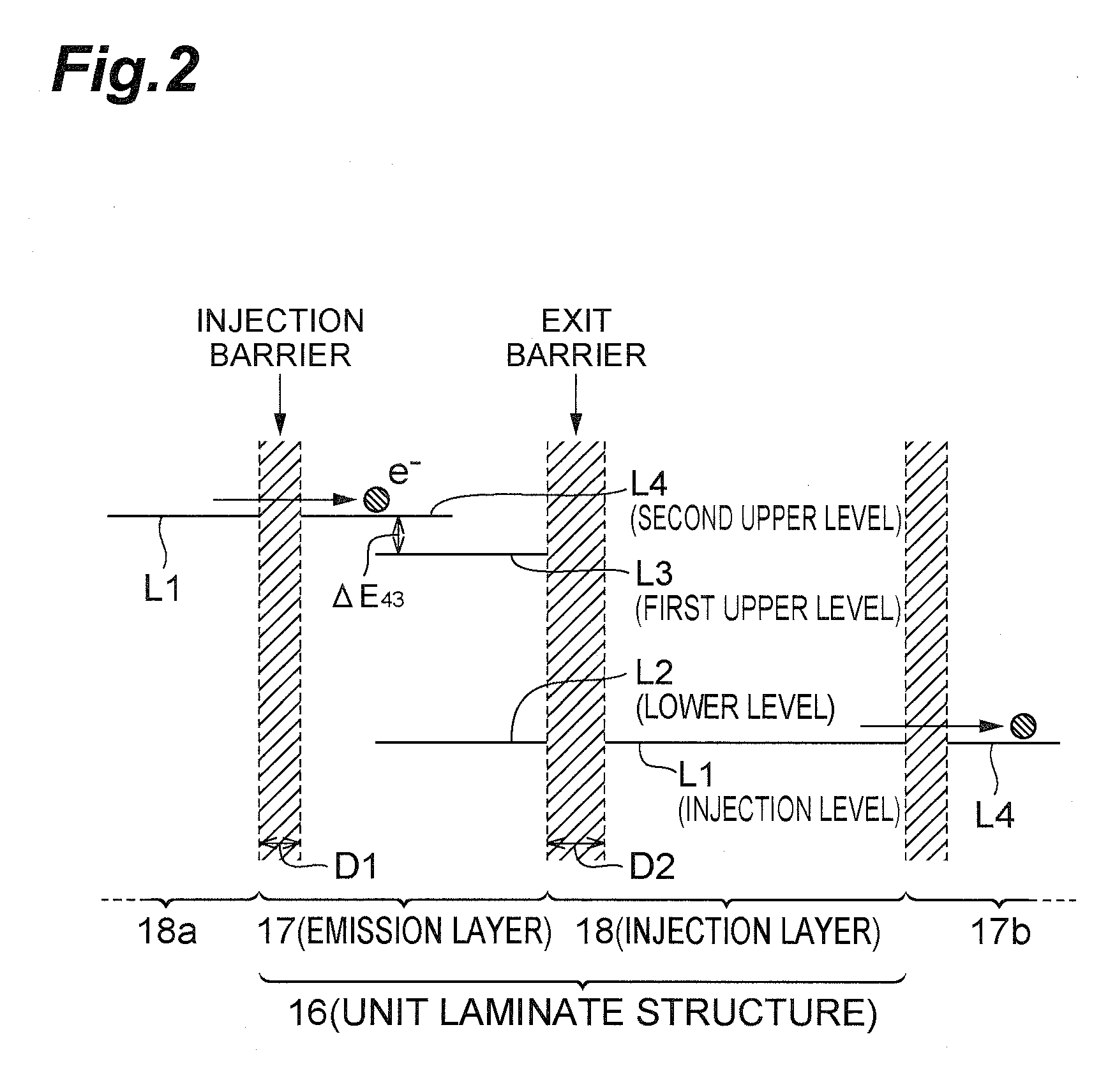
[0015]In addition, in the above level structure, the energy interval between the first upper level and the second upper level is set to be smaller than the energy of a longitudinal optical (LO) phonon. Accordingly, high-speed relaxation of electrons injected into the second upper level to the first upper level due to LO phonon scattering is prohibited. Further, the layer thickness of the exit barrier layer from the emission layer to the injection layer is set in a range not less than 70% and not more than 150% of the layer thickness of the injection barrier layer. By thus setting the layer thickness of the exit barrier layer thicker than ordinary, the tunneling time of electrons from the lower level in the emission layer to the injection level in the injection layer becomes longer, and electrons are present at the lower level at a high density.

Problems solved by technology

However, all of the conventional light emitting devices using polaritons described above use photoexcitation in a microcavity structure, and are not practical devices.
However, it is very difficult to realize current injection in a microcavity structure.

Method used


Image

  • Semiconductor light emitting device
  • Semiconductor light emitting device
  • Semiconductor light emitting device

Examples


Embodiment Construction

[0033]Hereinafter, preferred embodiments of a semiconductor light emitting device according to the present invention will be described in detail with reference to the drawings. In the description of the drawings, the same components are attached with the same reference symbols, and overlapping description will be omitted. Moreover, the dimensional ratios in the drawings are not always equal to those in the description.

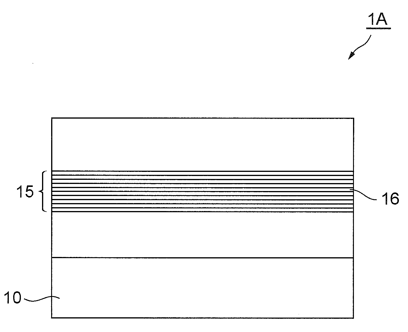
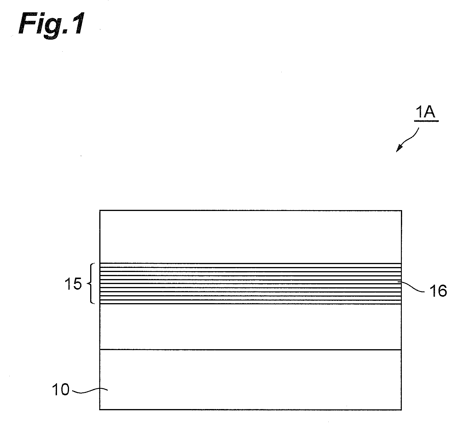
[0034]FIG. 1 is a view schematically showing a basic configuration of a semiconductor light emitting device according to the present invention. A semiconductor light emitting device 1A of the present embodiment is a monopolar type light emitting device which generates light by emission transition using a subband level structure in a semiconductor quantum well structure. This light emitting device 1A is especially configured as a novel semiconductor light emitting device using polaritons, and the emission structure thereof is characterized by a polariton generation stru...


PUM


Abstract

A semiconductor light emitting device including a semiconductor substrate and an active layer which is formed on the substrate and has a cascade structure formed by multistage-laminating unit laminate structures 16 each including an emission layer 17 and an injection layer 18 is configured. The unit laminate structure 16 has a first upper level L3, a second upper level L4, and a lower level L2 in the emission layer 17, and an injection level L1 in the injection layer 18, an energy interval between the levels L3 and L4 is set to be smaller than the energy of an LO phonon, the layer thickness of the exit barrier layer is set in a range not less than 70% and not more than 150% of the layer thickness of the injection barrier layer, light is generated by emission transition in the emission layer 17, and electrons after the emission transition are injected from the level L2 into the level L4 of the emission layer of a subsequent stage via the level L1. Accordingly, a semiconductor light emitting device using polaritons, capable of performing a light emitting operation by current injection, is realized.

Description

BACKGROUND OF THE INVENTION[0001]1. Field of the Invention[0002]The present invention relates to a semiconductor light emitting device which generates light by emission transition using a subband level structure in a quantum well structure.[0003]2. Related Background Art[0004]In a conventional semiconductor laser, limits of reduction of threshold and of reduction of power consumption are determined generally according to a carrier injection rate for forming a population inversion necessary for laser oscillation. As one of the methods for exceeding the limit, a method for configuring a light emitting device by using polaritons in a resonator is considered. In a light emitting device using polaritons, by Bose-Einstein condensation (BEC), coherent light can be generated with very few injected carriers without forming a population inversion.[0005]Here, polaritons are quasi-particles obtained by quantizing a coupled wave formed by strong coupling between an electron system and a photon s...

Claims


Application Information

Patent Timeline
IPC IPC(8): H01L33/04
CPCB82Y20/00H01S5/3402H01L33/06
Inventor EDAMURA, TADATAKAFUJITA, KAZUUEHIGUCHI, AKIRAAKIKUSA, NAOTAYAMANISHI, MASAMICHI
Owner HAMAMATSU PHOTONICS KK
Learn More